With the revenue from the Z80, the company built its own chip factories.[4] Zilog licensed the Z80 to the US-based Synertek and Mostek, which had helped them with initial production, as well as to a European second-source manufacturer SGS. The design was also copied by several Japanese, Eastern European and Soviet manufacturers.[lower-roman 3] This won the Z80 acceptance in the world market since large companies like NEC, Toshiba, Sharp, and Hitachi started to manufacture the device (or their own Z80-compatible clones or designs).
In later decades, the Z80 remained in use in embedded systems and continued to see improvements. The most recent Z80-compatible microcontroller family, the fully pipelined24-biteZ80 with a linear 16MBaddress range, has been sold alongside the simpler Z80 and Z180 products.
Zilog announced in April 2024 that it would begin discontinuing manufacture of the Z80 CPU after 48 years on the market.[5]
History
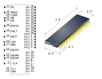
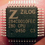
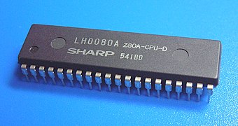
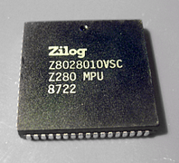
A May 1976 advertisement for the Z80 outlines its major advantages over the 8080.Photo of the original Zilog Z80 microprocessor design in depletion-load nMOS. Total die size is 3545×3350μm. The blue squares around the outside are the pads that connect to the external pins. This chip was manufactured in 1990.A CMOS Z80 in a 44-pin quad flat package.
In early 1974, Intel viewed their microprocessors not so much as products to be sold on their own but as a way to sell more of their main products, static RAM and ROM. A reorganization placed many of the formerly independent sections under the direction of Les Vadasz, further diluting the microprocessor's place in the company. That year, the 1973–1975 recession reached a peak and Intel laid off a number of employees.[6] All of this led to Faggin becoming restless, and he invited Ungermann out for drinks and asked if he would be interested in starting their own company. Ungermann immediately agreed, and as he had less to do at Intel, left in August or September, followed by Faggin, whose last day at Intel was Halloween 1974.[7] When Shima heard, he asked to come to the new company as well, but having no actual product design or money, they told him to wait.[8]
The newly formed and unnamed company initially began designing a single-chip microcontroller called the 2001. They met with Synertek to discuss fabrication on their lines, and when Faggin began to understand the costs involved it became clear that a low-cost product like this would not be able to compete with a design from a company with its own production lines, like Intel. They then began considering a more complex microprocessor instead, initially known as the Super 80, with the main feature being its use of a +5V bus[8] instead of the more common −5, +5 and 12V used by designs like the 8080. The new design was intended to be compatible with the 8080, but add many of the nice features of the Motorola 6800, including index registers and improved interrupts.[9]
Exxon investment, detailed development begins
While still being set up, the industry newsletter Electronic News heard of them and published a story on the newly formed company. This attracted the attention of Exxon Enterprises, Exxon's high-tech investment arm. At the time, in the midst of the recession, there was very little venture capital available, with a total of $10 million for the entire industry being spent in all of 1975 (equivalent to $57million in 2023). Someone from Exxon contacted the still-unnamed company,[8] and arranged a meeting that eventually led to them providing an initial $500,000 funding in June 1975 (equivalent to $2.8million in 2023).[10]
With funding being discussed, and a design to be built, Shima joined in February 1975.[9] Shima immediately set about producing a high-level design, adding several concepts of his own. In particular, he used his experience on NECminicomputers to add the concept of two sets of processor registers so they could quickly respond to interrupts.[7][lower-roman 4] Ungerman began the development of a series of related controllers and peripheral chips that would complement the design.[11]
Through this period, Shima developed a legendary reputation for being able to convert logic concepts into physical design in realtime; while discussing a proposed feature, he would often interrupt and state how much room that would take on the chip and veto its addition if it was too large.[12] The first pass at the design was complete by April 1975. Shima had completed a logic layout by the beginning of May. A second version of the logic design was issued on 7 August and the bus details by 16 September. Tape-out was completed in November and converting the tape into a production mask required two more months.[13]
Faggin had already started looking for a production partner. By this time, Synertek and Mostek had both set up the depletion-mode production lines that could be used to produce the design. Having talked to Synertek previously, Faggin approached them first. However, the president of Synertek demanded that the company be given a second source license, allowing them to sell the design directly. Faggin thought this would mean they could never compete even if they set up their own lines, and the agreement fell through. He then turned to Mostek, who agreed to a term of exclusivity while Zilog got their lines set up, and were eventually given the second source agreement.[14]
After considering many names for the new company, and finding them so unmemorable they could not recall them even a day later, Faggin and Ungermann were kicking around ideas based on "integrated logic" when Ungermann said "how about Zilog?" Faggin immediately agreed, stating they could say it was the "last word in integrated logic". When they met the next day and both immediately recalled it, the company had its name.[15]
Into production
The first samples were returned from Mostek on 9 March 1976.[11] By the end of the month, they had also completed an assembler-based development system. Some of the Z80 support and peripheral ICs were under development at this point, and many of them were launched during the following year. Among them were the Z80 CTC (counter/timer), Z80 DMA[16] (direct memory access), Z80 DART (dual asynchronous receiver–transmitter), Z80 SIO (synchronous communication controller), and Z80 PIO (parallel input/output).
The Z80 was officially launched in July 1976.[17] One of the first customers was a buyer who, unknown to Zilog, worked for NEC. At the time, the Japanese electronics companies were well known for taking US chip designs and producing them without a license. The Zilog team had worried about this, and Faggin had come up with the idea of adding transistors that would be subtly modified to operate differently than a visual inspection would suggest. Shima added six of these "traps" around the design. Sometime later, Shima was told by an engineer within NEC that the traps had delayed their copying efforts by six months.[18]
The successful launch allowed Faggin and Ungermann to approach Exxon looking for funding to build their own fab. The company agreed, and Zilog built a production line very rapidly. This allowed them to capture about 60 to 70% of the total market for Z80 sales.[19] With their own line running, Mostek was given the go-ahead to start sales of their own versions, the MK3880, which provided a second-source for customers which Intel lacked. At the time, a second-source was considered extremely important as a start-up like Zilog might go out of business and leave potential customers stranded.[9][lower-roman 5]
Comparison with the 8080
Faggin designed the instruction set to be binary compatible with the 8080[20][21] so that most 8080 code, notably the CP/Moperating system and Intel's PL/M compiler for 8080 (as well as its generated code), would run unmodified on the new Z80 CPU. Masatoshi Shima designed most of the microarchitecture as well as the gate and transistor levels of the Z80 CPU, assisted by a small number of engineers and layout people.[22][23] CEO Federico Faggin was actually heavily involved in the chip layout work, together with two dedicated layout people. According to Faggin, he worked 80hours a week in order to meet the tight schedule given by the financial investors.[4]
The Z80 offered many improvements over the 8080:[21]
A more automatic and general vectorized interrupt system, mode2, primarily intended for Zilog's line of counter/timers, DMA and communications controllers, as well as a fixed vector interrupt system, mode1, for simple systems with minimal hardware (with mode0 being the 8080-compatible mode).[25]
A non-maskable interrupt (NMI), which can be used to respond to power-down situations or other high-priority events (and allowing a minimalistic Z80 system to easily implement a two-level interrupt scheme in mode1).
A complete duplicate register file,[26] which could be quickly switched, to speed up response to interrupts such as fast asynchronous event handlers or a multitaskingdispatcher. Although they were not intended as extra registers for general code, they were nevertheless used that way in some applications.[lower-roman 7]
Less hardware required for power supply, clock generation and interface to memory and I/O
Single 5-volt power supply (the 8080 needed −5V, +5V, and +12V).
Single-phase 5-volt clock (the 8080 needed a high-amplitude (9 to 12volts) non-overlapping two-phase clock).
Built-in DRAMrefresh, which would otherwise require external circuitry, unless SRAM, more expensive and less dense (but faster), was used.[lower-roman 8]
Non-multiplexed buses (the 8080 had state signals multiplexed onto the data bus).
A special reset that zeroes only the program counter, so that a single Z80 CPU could be used in a development system such as an in-circuit emulator.[27]
Success in the market
The Z80 took over from the 8080 and its offspring, the 8085, in the processor market[28] and became one of the most popular and widely used 8-bit CPUs.[2][3] Some organizations such as British Telecom remained loyal to the 8085 for embedded applications, owing to their familiarity with it and to its on-chip serial interface and interrupt architecture. Likewise, Zenith Data Systems paired the 8085 with the 16-bit Intel 8088 in its first MS-DOS computer, the Zenith Z-100, despite having previous experience with its pioneering Z80-based HeathkitH89 and ZenithZ-89 products. However, other computers were made integrating the Z80 with other CPUs: the Radio Shack TRS-80 Model16 with a Motorola 68000, the DEC Rainbow with an 8088, and the Commodore 128 with a MOS 8502.
Zilog was later producing a low-power Z80 suitable for the growing laptop computer market of the early 1980s. Intel produced a CMOS 8085 (80C85) used in battery-powered portable computers, such as the Kyocera-designed laptop from April 1983, also sold by Tandy (as TRS-80 Model 100), Olivetti, and NEC. In following years, however, CMOS versions of the Z80 (from both Zilog and Japanese manufacturers) would dominate this market as well, in products such as the Amstrad NC100, Cambridge Z88 and Tandy's own WP-2.
Perhaps a key to the initial success of the Z80 was the built-in DRAM refresh, at least in markets such as CP/M and other office and home computers. (Most Z80 embedded systems use static RAM that do not need refresh.) It may also have been its minimalistic two-level interrupt system, or conversely, its general multi-level daisy-chain interrupt system useful in servicing multiple Z80 IO chips. These features allowed systems to be built with less support hardware and simpler circuit board layouts.
However, others claim that its popularity was due to the duplicated registers that allowed fast context switches or more efficient processing of things like floating-point math compared to 8-bit CPUs with fewer registers. (The Z80 can keep several such numbers internally, using HL'HL, DE'DE and BC'BC as 32-bits registers, avoiding having to access them from slower RAM during computation.)[29]
For the original NMOS design, the specified upper clock-frequency limit increased successively from the introductory 2.5MHz, via the well known 4MHz (Z80A), up to 6 (Z80B) and 8MHz (Z80H).[30][31] The NMOS version has been produced as a 10MHz part since the late 1980s. CMOS versions were developed with specified upper frequency limits ranging from 4MHz up to 20MHz for the version sold today. The CMOS versions allowed low-power standby with internal state retained, having no lower frequency limit.[lower-roman 9] The fully compatible derivatives HD64180/Z180[32][33] and eZ80 are currently specified for up to 33 and 50MHz respectively.
Design
Programming model and register set
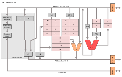
An approximate block diagram of the Z80: There is no dedicated adder for offsets or separate incrementer for R, and no need for more than a single 16-bit temporary register WZ (although the incrementer latches are also used as a 16-bit temporary register, in other contexts). It is the PC and IR registers that are placed in a separate group, with a detachable bus segment, to allow updates of these registers in parallel with the main register bank.
The programming model and register set of the Z80 are fairly conventional, ultimately based on the register structure of the Datapoint 2200. The Z80 was designed as an extension of the Intel 8080, created by the same engineers, which in turn was an extension of the 8008. The 8008 was basically a PMOS implementation of the TTL-based CPU of the Datapoint 2200.[lower-roman 10]
The 2200 design allowed 8-bit registers H and L (High and Low) to be paired into a 16-bit address register HL.[lower-roman 11] In the 8080, this pairing was added to the BC and DE pairs as well, while HL was generalized to allow use as a 16-bit accumulator, not just an address register. The 8080 also introduced immediate 16-bit data for BC, DE, HL, and SP loads. Furthermore, direct 16-bit copying between HL and memory was now possible, using a direct address.
The Z80 orthogonalized this further by making all 16-bit register pairs, including IX and IY, more general purpose, as well as allowing 16-bit copying directly to and from memory for all of these pairs. The 16-bit IX and IY registers in the Z80 are primarily intended as base address-registers, where a particular instruction supplies a constant offset that is added to the previous values, but they are also usable as 16-bit accumulators, among other things. A limitation is that all operand references involving IX or IY require an extra instruction prefix byte, adding at least four clock cycles over the timing of an instruction using HL instead; this sometimes makes using IX or IY less efficient than a method using only the 8080-model registers. The Z80 also introduced a new signed overflow flag and complemented the fairly simple 16-bit arithmetics of the 8080 with dedicated instructions for signed 16-bit arithmetics.
The 8080-compatible registers AF, BC, DE, HL are duplicated as a separate register file in the Z80,[35] where the processor can quickly (four t-states, the least possible execution time for any Z80 instruction) switch from one bank to the other;[36] a feature useful for speeding up responses to single-level, high-priority interrupts. A similar feature was present in the 2200, but was never implemented at Intel. The dual register-set is very useful in the embedded role, as it improves interrupt handling performance, but found widespread use in the personal computer role as an additional set of general registers for complex code like floating-point arithmetic or home computer games.
The duplicate register file is often referred to as the "alternate register set" (by some, the "primed" register file since the apostrophe character is used to denote them in assembler source code and the Zilog documentation). This emphasizes that only one set is addressable at any time. However, the 8-bit accumulator A with its flag register F is bifurcated from the "general purpose" register pairs HL, DE and BC. This is accomplished with two separate instructions used to swap their accessibilities: EX AF,AF' exchanges only register pair AF with AF', while the EXX instruction exchanges the three general purpose register pairs HL, DE and BC with their alternates HL', DE' and BC'. Thus the accumulator A can interact independently with any of the general purpose 8-bit registers in the alternate (or primed) register file, or, if HL' contains a pointer to memory, some byte there (DE' and BC' can also transfer 8-bit data between memory and accumulator A).
This can become confusing for programmers because after executing EX AF,AF' or EXX what were previously the alternate (primed) registers are now the main registers, and vice versa. The only way for the programmer to tell which set(s) are in context (while "playing computer" while scrutinizing the assembler source text, or worse, poring over code with a debugger) is to trace where each register swap is made at each point in the program. Obviously if many jump and calls are made within these code segments it can quickly become difficult to tell which register file is in context unless carefully commented. Thus it is advisable that exchange instructions be used directly and in short discrete code segments. The Zilog Z280 instruction set includes JAF and JAR instructions which jump to a destination address if the alternate registers are in context (thus officially recognizing this programming complication).
As on the 8080, 8-bit registers are typically paired to provide 16-bit versions. The 8080 compatible registers[37] are:
AF: 8-bit accumulator (A) and flag bits (F) carry, zero, minus, parity/overflow, half-carry (used for BCD), and an Add/Subtract flag (usually called N) also for BCD
BC: 16-bit data/address register or two 8-bit registers
DE: 16-bit data/address register or two 8-bit registers
HL: 16-bit accumulator/address register or two 8-bit registers
IX: 16-bit index or base register for 8-bit immediate offsets
IY: 16-bit index or base register for 8-bit immediate offsets
I: interrupt vector base register, 8 bits
R: DRAM refresh counter, 8 bits (msb does not count)
AF': alternate (or shadow) accumulator and flags (toggled in and out with EX AF,AF' )
BC', DE' and HL': alternate (or shadow) registers (toggled in and out with EXX)
Four bits of interrupt status and interrupt mode status
The refresh register, R, increments each time the CPU fetches an opcode (or an opcode prefix, which internally executes like a 1-byte instruction) and has no simple relationship with program execution. This has sometimes been used to generate pseudorandom numbers in games, and also in software protection schemes.[citation needed] It has also been employed as a "hardware" counter in some designs; an example of this is the ZX81, which lets it keep track of character positions on the TV screen by triggering an interrupt at wrap around (by connecting INT to A6).
The interrupt vector register, I, is used for the Z80 specific mode 2 interrupts (selected by the IM 2 instruction). It supplies the high byte of the base address for a 128-entry table of service routine addresses which are selected via an index sent to the CPU during an interrupt acknowledge cycle; this index is simply the low byte part of the pointer to the tabulated indirect address pointing to the service routine.[25] The pointer identifies a particular peripheral chip or peripheral function or event, where the chips are normally connected in a so-called daisy chain for priority resolution. Like the refresh register, this register has also sometimes been used creatively; in interrupt modes 0 and 1 (or in a system not using interrupts) it can be used as simply another 8-bit data register.
The instructions LD A,R and LD A,I affect the Z80 flags register, unlike all the other LD (load) instructions. The Sign (bit 7) and Zero (bit 6) flags are set according to the data loaded from the Refresh or Interrupt source registers. For both instructions, the Parity/Overflow flag (bit 2) is set according to the current state of the IFF2 flip-flop.[38]
Microarchitecture
Although the Z80 is generally considered an eight-bit CPU, it has a four-bit ALU, so calculations are done in two steps for 8-bit quantities and four steps for 16-bit quantities (such as ADD HL,DE, ADC HL,DE, etc.).[39]
Z80 assembly language
Datapoint 2200 and Intel 8008
The first Intel 8008 assembly language was based on a very simple (but systematic) syntax inherited from the Datapoint 2200 design. This original syntax was later transformed into a new, somewhat more traditional, assembly language form for this same original 8008 chip. At about the same time, the new assembly language was also extended to accommodate the additional addressing modes in the more advanced Intel 8080 chip (the 8008 and 8080 shared a language subset without being binary compatible; however, the 8008 was binary compatible with the Datapoint 2200).
In this process, the mnemonic L, for LOAD, was replaced by various abbreviations of the words LOAD, STORE and MOVE, intermixed with other symbolic letters. The mnemonic letter M, for memory (referenced by HL), was lifted out from within the instruction mnemonic to become a syntactically freestanding operand, while registers and combinations of registers became very inconsistently denoted; either by abbreviated operands (MVI D, LXI H and so on), within the instruction mnemonic itself (LDA, LHLD and so on), or both at the same time (LDAX B, STAX D and so on).
Intel8008 Datapoint2200
Intel8080 Intel8085
ZilogZ80
Intel8086/ Intel8088
before ca. 1973
ca. 1974
1976
1978
LBC
MOVB,C
LDB,C
MOVCH,CL
--
LDAXB
LDA,(BC)
--
LAM
MOVA,M
LDA,(HL)
MOVAL,[BX]
LBM
MOVB,M
LDB,(HL)
MOVCH,[BX]
--
STAXD
LD(DE),A
--
LMA
MOVM,A
LD(HL),A
MOV[BX],AL
LMC
MOVM,C
LD(HL),C
MOV[BX],CL
LDI56
MVID,56
LDD,56
MOVDL,56
LMI56
MVIM,56
LD(HL),56
MOVbyteptr[BX],56
--
LDA1234
LDA,(1234)
MOVAL,[1234]
--
STA1234
LD(1234),A
MOV[1234],AL
--
--
LDB,(IX+56)
MOVCH,[SI+56]
--
--
LD(IX+56),C
MOV[SI+56],CL
--
--
LD(IY+56),78
MOVbyteptr[DI+56],78
--
LXIB,1234
LDBC,1234
MOVCX,1234
--
LXIH,1234
LDHL,1234
MOVBX,1234
--
SHLD1234
LD(1234),HL
MOV[1234],BX
--
LHLD1234
LDHL,(1234)
MOVBX,[1234]
--
--
LDBC,(1234)
MOVCX,[1234]
--
--
LDIX,(1234)
MOVSI,[1234]
Illustration of four syntaxes, using samples of equivalent, or (for 8086) very similar, load and store instructions.[40] The Z80 syntax uses parentheses around an expression to indicate that the value should be used as a memory address (as mentioned below), while the 8086 syntax uses brackets instead of ordinary parentheses for this purpose. Both Z80 and 8086 use the + sign to indicate that a constant is added to a base register to form an address. Note that the 8086 is not a complete superset of the Z80. BX is the only 8086 register pair that can be used as a pointer.
New syntax
Because Intel claimed a copyright on their assembly mnemonics,[41] a new assembly syntax had to be developed for the Z80. This time a more systematic approach was used:
All registers and register pairs are explicitly denoted by their full names
Parentheses are consistently used to indicate "memory contents at" (constant address or variable pointer dereferencing) with the exception of one jump instruction JP (HL). JP (XY) is merely a variation of JP (HL) loading the new PC address. [lower-roman 12]
All load and store instructions use the same mnemonic name, LD, for LOAD (a return to the simplistic Datapoint 2200 vocabulary); other common instructions, such as ADD and INC, use the same mnemonic regardless of addressing mode or operand size. This is possible because the operands themselves carry enough information.
These principles made it straightforward to find names and forms for all new Z80 instructions, as well as orthogonalizations of old ones, such as LD BC,(1234).
Apart from naming differences, and despite a certain discrepancy in basic register structure, the Z80 and 8086 syntax are virtually isomorphic for a large portion of instructions. Only quite superficial similarities (such as the word MOV, or the letter X, for extended register) exist between the 8080 and 8086 assembly languages, although 8080 programs can be translated to 8086 assembly language by translator programs.[43][44]
Instruction set and encoding
The Z80 uses 252 out of the available 256 codes as single byte opcodes ("root instruction" most of which are inherited from the 8080); the four remaining codes are used extensively as opcode prefixes:[45] CB and ED enable extra instructions, and DD or FD select IX+d or IY+d respectively (in some cases without displacement d) in place of HL. This scheme gives the Z80 a large number of permutations of instructions and registers; Zilog categorizes these into 158 different "instruction types", 78 of which are the same as those of the Intel 8080[45] (allowing operation of all 8080 programs on a Z80). The Zilog documentation[46] further groups instructions into the following categories (most from the 8080, others entirely new like the block and bit instructions, and others 8080 instructions with more versatile addressing modes, like the 16-bit loads, I/O, rotates/shifts and relative jumps):
Load and exchange
Block transfer and search
Arithmetic and logical
Rotate and shift
Bit manipulation (set, reset, test)
Jump, call and return
Input/output
Basic CPU control
No explicit multiply instructions are available in the original Z80,[47] though registers A and HL can be multiplied by powers of two with ADDA,A and ADDHL,HL instructions (similarly IX and IY also). Shift instructions can also multiply or divide by powers of two.
Different sizes and variants of additions, shifts, and rotates have somewhat differing effects on flags because most of the flag-changing properties of the 8080 were copied. However, the parity flag bitP of the 8080 (bit2) is called P/V (parity/overflow) in the Z80 as it serves the additional purpose of a twos complement overflow indicator, a feature lacking in the 8080. Arithmetic instructions on the Z80 set it to indicate overflow rather than parity, while bitwise instructions still use it as a parity flag. (This introduces a subtle incompatibility of the Z80 with code written for the 8080, as the Z80 sometimes indicates signed overflow where the 8080 would indicate parity, possibly causing the logic of some practical 8080 software to fail on the Z80.[lower-roman 13]) This new overflow flag is used for all new Z80-specific 16-bit operations (ADC, SBC) as well as for 8-bit arithmetic operations, while the 16-bit operations inherited from the 8080 (ADD, INC, DEC) do not affect it. Also, bit1 of the flags register (a spare bit on the 8080) is used as a flagN that indicates whether the last arithmetic instruction executed was a subtraction or addition. The Z80 version of the DAA instruction (decimal adjust accumulator for BCD arithmetic) checks the Nflag and behaves accordingly, so a (hypothetical) subtraction followed later by DAA will yield a different result on an old 8080 than on the Z80. However, this would likely be erroneous code on the 8080, as DAA was defined for addition only on that processor.
The Z80 has six new LD instructions that can load the DE, BC, and SP register pairs from memory, and load memory from these three register pairs—unlike the 8080.[40] As on the 8080, load instructions do not affect the flags (except for the special-purpose I and R register loads). A result of a regular encoding (common with the 8080) is that each of the 8-bit registers can be loaded from themselves (e.g. LD A,A). This is effectively a NOP.
New block transfer instructions can move up to 64kilobytes from memory to memory or between memory and I/O peripheral ports. Block instructions LDIR and LDDR (load, increment/decrement, repeat) use HL to point to the source address, DE to the destination address, and BC as a byte counter. Bytes are copied from source to destination, the pointers are incremented or decremented, and the byte counter is decremented until BC reaches zero. Non-repeating versions LDI and LDD move a single byte and bump the pointers and byte counter, which if it becomes zero resets the P/Vflag. Corresponding memory-to-I/O instructions INIR, INDR, OTIR, OTDR, INI, IND, OUTI and OUTD operate similarly, except that B, not BC, is used as the byte counter.[48][49] The Z80 can input and output any register to an I/O port using registerC to designate the port. (The 8080 only performs I/O through the accumulatorA, using a direct port address specified in the instruction; a self-modifying code technique is required to use a variable 8080 port address.)
The last group of block instructions perform a CP compare operation between the byte at (HL) and the accumulatorA. Register pair DE is not used. The repeating versions CPIR and CPDR only terminate if BC goes to zero or a match is found. HL is left pointing to the byte after (CPIR) or before (CPDR) the matching byte. If no match is found the Zflag is reset. There are non-repeating versions CPI and CPD.
Unlike the 8080, the Z80 can jump to a relative address (JR instead of JP) using a signed 8-bit displacement. Only the zero and carry flags can be tested for these new two-byte JR instructions. (All 8080 jumps and calls, conditional or not, are three-byte instructions.) A two-byte instruction specialized for program looping is also new to the Z80: DJNZ (decrement jump if non-zero) takes a signed 8-bit displacement as an immediate operand. The Bregister is decremented, and if the result is nonzero, then program execution jumps relative to PC; the flags remain unaltered. To perform an equivalent loop on an 8080 requires separate DEC and conditional jump (to a two-byte absolute address) instructions (totalling four bytes), and the DEC alters the flag register.
The index register (IX/IY, often abbreviated XY) instructions can be useful for accessing data organised in fixed heterogenous structures (such as records) or at fixed offsets relative a variable base address (as in recursivestack frames) and can also reduce code size by removing the need for multiple short instructions using non-indexed registers. However, although they may save speed in some contexts when compared to long/complex "equivalent" sequences of simpler operations, they incur a lot of additional CPU time (e.g., 19 T-states to access one indexed memory location vs. as little as 11 to access the same memory using HL and INC to point to the next). Thus, for simple or linear accesses of data, use of IX and IY tend to be slower and occupy more memory. Still, they may be useful in cases where the "main" registers are all occupied, by removing the need to save/restore registers. Their officially undocumented 8-bit halves (see below) can be especially useful in this context, for they incur less slowdown than their 16-bit parents. Similarly, instructions for 16-bit additions are not particularly fast (11clocks) in the original Z80 (being 1clock slower than in the 8080/8085); nonetheless, they are about twice as fast as performing the same calculations using 8-bit operations, and equally important, they reduce register usage. It was not uncommon for programmers to "poke" different offset displacement bytes (which were typically calculated dynamically) into indexed instructions; this is an example of self-modifying code, which was regular practice on nearly all early 8-bit processors with non-pipelined execution units.
The index registers have a parallel instruction to JP (HL), which is JP (XY). This is often seen in stack-oriented languages like Forth, which at the end of every Forth word (atomic subroutines comprising the language) must jump unconditionally back to their thread interpreter routines. Typically this jump instruction appears many hundreds of times in an application, and using JP (XY) rather than JP THREAD saves a byte and two T-states for each occurrence. This naturally makes the index register unavailable for any other use, or else the need to constantly reload it would negate its efficiency.
The 10-year-newer microcoded Z180 design could initially afford more "chip area", permitting a slightly more efficient implementation (using a wider ALU, among other things); similar things can be said for the Z800, Z280, and Z380. However, it was not until the fully pipelined eZ80 was launched in 2001 that those instructions finally became approximately as cycle-efficient as it is technically possible to make them, i.e. given the Z80 encodings combined with the capability to do an 8-bit read or write every clock cycle.[citation needed]
Undocumented instructions
The index registers, IX and IY, were intended as flexible 16-bit pointers, enhancing the ability to manipulate memory, stack frames and data structures. Officially, they were treated as 16-bit only. In reality they were implemented as a pair of 8-bit registers,[50] in the same fashion as the HL register, which is accessible either as 16 bits or separately as the High and Low registers. The binary opcodes (machine language) were identical, but preceded by a new opcode prefix.[51] Zilog published the opcodes and related mnemonics for the intended functions, but did not document the fact that every opcode that allowed manipulation of the H and L registers was equally valid for the 8 bit portions of the IX and IY registers. For example, the opcode 26h followed by an immediate byte value (LD H,n) will load that value into the H register. Preceding this two-byte instruction with the IX register's opcode prefix, DD, would instead result in the most significant 8 bits of the IX register being loaded with that same value. A notable exception to this would be instructions similar to LD H,(IX+d) which make use of both the HL and IX or IY registers in the same instruction;[51] in this case the DD prefix is only applied to the (IX+d) portion of the instruction. The halves of the XY registers could also hold operands for 8-bit arithmetic, logical and compare instructions, sparing the regular 8-bit registers for other use. The undocumented ability to increment and decrement the upper half of an index register made it easy to expand the range of the normal indexed instructions, without having to resort to the documented ADD/SBC XY,DE or ADD/SBC XY,BC.
There are several other undocumented instructions as well.[52] Undocumented or illegal opcodes are not detected by the Z80 and have various effects, some of which are useful. However, as they are not part of the formal definition of the instruction set, different implementations of the Z80 are not guaranteed (or especially likely) to work the same way for every undocumented opcode.
Bugs
The OTDR instruction does not conform to the Z80 documentation. Both the OTDR and OTIR instructions are supposed to leave the carry (C) flag unmodified. The OTIR instruction operates correctly; however, during the execution of the OTDR instruction, the carry flag takes the results of a spurious compare between the accumulator (A) and the last output of the OTDR instruction.[53]
Example code
EXAMPLE 1: The following Z80 assembler source code is for a subroutine named HELLO_WORLD. This is an introductory program which will print a message to the video display and then exit. Though simple, it demonstrates how an assembler source code is formatted and interacts with the display hardware through a computer operating system. This is necessarily specific to a particular computer hardware, operating system and assembler software. The example used is the TRS-80 Model 4 running TRSDOS/LS-DOS 6.x, produced by Tandy/Radio Shack and Logical Systems, with most any assembler sold by Radio Shack or Misosys Inc. (Series I/EDTASM, ALDS, EDAS or MRAS with -GC switch). The principal features of this configuration are universal to Z80 assemblers, even under CP/M.
3000 3E 69 3002 EF 3003 21 14 30 3006 3E 0A 3008 EF 3009 0E 0D 300B 3E 02 300D EF 300E 21 00 00 3011 3E 16 3013 EF 3014 48 65 6C 6C 3018 6F 2C 20 77 301C 6F 72 6C 64 3020 21 0D 0D 3023
; hello_world_TRS-80 Model 4; Print "Hello, world!" then exit to TRSDOS Ready;; Entry registers: none; Return registers: none;; values below are decimal unless suffixed by H; the term "pseudo-op" means same as "assembler directive", is not Z80 code;@CLSEQU105; EQU pseudo-op sets @CLS text label = TRSDOS Supervisor Code@DSPEQU2; set @DSP text label = TRSDOS SVC to send char to display@DSPLYEQU10; set @DSPLY text label = SVC for text string display@EXITEQU22; set @EXIT text label = SVC for returning to TRSDOS Ready;ORG3000H; ORG pseudo-op sets standard start address under TRSDOS 6.xSTARTLDA,@CLS; CLS = Clear Screen, erase display and home cursorRST40; Z80 Restart instruction for system SVC processor, execute @CLSLDHL,MSG; point to message string with HL (required by @DSPLY SVC)LDA,@DSPLY; send text string to *DO Display Output device (video screen)RST40; execute @DSPLY SVC (13d byte needed to terminate string)LDC,13; now send another carriage return, needed in reg C LDA,@DSP; to set off Hello message from TRSDOS Ready promptRST40; once we exit to systemLDHL,0; indicate no error condition to Command InterpreterLDA,@EXIT; return to TRSDOS ReadyRST40; (stack integrity maintained, could as well have used a RET!)MSGDB'Hello, world!',13; DB = Define Byte pseudo-op assembles ASCII string to Z80 memoryCRDB13; 13d byte is ASCII carriage return char, moves cursor downENDSTART; END pseudo-op required by assembler ; to produce transfer record to program entry point
EXAMPLE 2: The following Z80 assembly source code is for a subroutine named memcpy that copies a block of data bytes of a given size from one location to another. Important: the example code does not handle the case where the destination block overlaps the source; a serious limitation, but one that is irrelevant for some applications—such as, especially, when the source is in ROM and the destination in RAM, so they can never overlap. The data block is copied one byte at a time, and the data movement and looping logic utilizes 16-bit operations. It demonstrates a variety of instructions but in practice it would not be coded this way as the Z80 has a single instruction that will replace this entire subroutine: LDIR. The sample code will move one byte every 46 T-states. Substituting the LDIR instruction will move each byte in only 21 T-states. Note that the assembled code is binary-compatible with the Intel 8080 and 8085 CPUs.
; memcpy --; Copy a block of memory from one location to another.; This routine is the equivalent of LDIR ;; Entry registers; HL - Address of source data block; DE - Address of destination data block; BC - Number of bytes to copy;; Return registers; HL - First byte after source data block; DE - First byte after destination data block; BC - Zeroorg1000h;Origin at 1000hmemcpypublicpushaf;Save AF like LDIRlooplda,(hl);Load source byteld(de),a;save itinchl;Bump source pointerincde;Bump dest pointerdecbc;Bump counterlda,b;Test BC for zeroorc;If BC = 0,jpnz,loop;Repeat the looppopafretend
Instruction execution
Each instruction is executed in steps that are usually termed machine cycles (M-cycles), each of which can take between three and six clock periods (T-states).[54] Each M-cycle corresponds roughly to one memory access or internal operation. Many instructions actually end during the M1 of the next instruction which is known as a fetch/execute overlap.
Examples of typical instructions (R=read, W=write)
The Z80 machine cycles are sequenced by an internal state machine which builds each M-cycle out of 3, 4, 5 or 6 T-states depending on context. This avoids cumbersome asynchronous logic and makes the control signals behave consistently at a wide range of clock frequencies. It also means that a higher frequency crystal must be used than without this subdivision of machine cycles (approximately 2–3 times higher). It does not imply tighter requirements on memory access times, since a high resolution clock allows more precise control of memory timings and so memory can be active in parallel with the CPU to a greater extent, allowing more efficient use of available memory bandwidth.[citation needed]
One central example of this is that, for opcode fetch, the Z80 combines two full clock cycles into a memory access period (the M1-signal). In the Z80 this signal lasts for a relatively larger part of the typical instruction execution time than in a design such as the 6800, 6502, or similar, where this period would typically last typically 30-40% of a clock cycle.[citation needed] With memory chip affordability (i.e. access times around 450-250ns in the 1980s[citation needed]) typically determining the fastest possible access time, this meant that such designs were locked to a significantly longer clock cycle (i.e. lower internal clock speed) than the Z80.
Memory was generally slow compared to the state machine sub-cycles (clock cycles) used in contemporary microprocessors. The shortest machine cycle that could safely be used in embedded designs has therefore often been limited by memory access times, not by the maximum CPU frequency (especially so during the home computer era). However, this relation has slowly changed during the last decades, particularly regarding SRAM; cacheless, single-cycle designs such as the eZ80 have therefore become much more meaningful recently.
The content of the refresh register R is sent out on the lower half of the address bus along with a refresh control signal while the CPU is decoding and executing the fetched instruction. During refresh the contents of the Interrupt register I are sent out on the upper half of the address bus.[61]
Compatible peripherals
Zilog introduced a number of peripheral parts for the Z80, which all support the Z80's interrupt handling system and I/O address space. These include the counter/timer channel (CTC),[62] the SIO (serial input/output), the DMA (direct memory access), the PIO (parallel input/output) and the DART (dual asynchronous receiver–transmitter). As the product line developed, low-power, high-speed and CMOS versions of these chips were introduced.
PIO Z84C2008
CTC Z84C3008
SIO Z84C4008
Like the 8080, 8085 and 8086 processors, but unlike processors such as the Motorola 6800 and MOS Technology 6502, the Z80 and 8080 has a separate control line and address space for I/O instructions. While some Z80-based computers such as the Osborne 1 used "Motorola-style" memory mapped input/output devices, usually the I/O space was used to address one of the many Zilog peripheral chips compatible with the Z80. During the timing for an I/O read or an I/O write operation, a single wait cycle is automatically inserted by the Z80.[63] Zilog I/O chips supported the Z80's new mode 2 interrupts which simplified interrupt handling for large numbers of peripherals.
The Z80 was officially described as supporting 16-bit (64KB) memory addressing, and 8-bit (256 ports) I/O-addressing. All I/O instructions actually assert the entire 16-bit address bus. OUT(C),reg and INreg,(C) places the contents of the entire 16-bit BC register on the address bus;[53] OUT(n),A and INA,(n) places the contents of the Aregister on b8–b15 of the address bus and n on b0–b7 of the address bus. A designer could choose to decode the entire 16-bit address bus on I/O operations in order to take advantage of this feature, or use the high half of the address bus to select subfeatures of the I/O device. This feature has also been used to minimise decoding hardware requirements, such as in the Amstrad CPC/PCW and ZX81.
Second sources and derivatives
Second sources
Mostek, which produced the first Z80 for Zilog, offered it as second-source as MK3880. SGS-Thomson (now STMicroelectronics) was a second-source, too, with their Z8400. Sharp and NEC developed second sources for the NMOS Z80, the LH0080 and μPD780C, respectively. The LH0080 was used in various home computers and personal computers made by Sharp and other Japanese manufacturers, including SonyMSX computers, and a number of computers in the Sharp MZ series.[64] Sharp developed the LH0080A and LH0080B to operate at frequencies of 4MHz and 6MHz, respectively.[65] Sharp also developed LH0083[66] compatible with Z80 DMA.
Toshiba made a CMOS-version, the TMPZ84C00, which is believed[by whom?] (but not verified) to be the same design also used by Zilog for its own CMOS Z84C00. There were also Z8400, Z80-chips made by GoldStar (now LG) and the BU18400 series of Z80-clones (including DMA, PIO, CTC, DART and SIO) in NMOS and CMOS made by ROHM Electronics. The LH5080,[67] LH5081,[68] and LH5082,[69] which are CMOS versions of the Z80, PIO, and CTC respectively, are manufactured by Sharp.
In East Germany, an unlicensed clone of the Z80, known as the U880, was manufactured. It was used extensively in Robotron's and VEB Mikroelektronik Mühlhausen's computer systems (such as the KC85-series) and also in many self-made computer systems. In Romania another unlicensed clone could be found, named MMN80CPU and produced by Microelectronica, used in home computers like TIM-S, HC, COBRA.
Also, several clones of Z80 were created in the Soviet Union, notable ones being the T34BM1, also called КР1858ВМ1 (parallelling the Soviet 8080-clone KR580VM80A). The first marking was used in pre-production series, while the second had to be used for a larger production. Though, due to the collapse of Soviet microelectronics in the late 1980s, there are many more T34BM1s than КР1858ВМ1s.[citation needed]
Hitachi developed the HD64180, a microcoded and partially dynamic Z80 in CMOS, with on chip peripherals and a simple MMU giving a 1MB address space. It was later second sourced by Zilog, initially as the Z64180, and then in the form of the slightly modified Z180[70] which has bus protocol and timings better adapted to Z80 peripheral chips. Z180 has been maintained and further developed under Zilog's name, the newest versions being based on the fully static S180/L180 core with very low power draw and EMI (noise).
Toshiba developed the 84 pin Z84013 / Z84C13 and the 100 pin Z84015 / Z84C15 series of "intelligent peripheral controllers", basically ordinary NMOS and CMOS Z80 cores with Z80 peripherals, watchdog timer, power on reset, and wait state generator on the same chip. Manufactured by Sharp as well as Toshiba. These products are today second sourced by Zilog.[71]
The 32-bit Z80 compatible Zilog Z380, introduced 1994, is used in telecom equipment.[72]
Zilog's fully pipelined Z80 compatible eZ80[73] with an 8/16/24-bit word length and a linear 16MB address space was introduced in 2001. It exists in versions with on chip SRAM or flash memory, as well as with integrated peripherals. One variant has on chip MAC (media access controller), and available software include a TCP/IP stack. In contrast with the Z800 and Z280, there are only a few added instructions (primarily LEAs, PEAs, and variable-address 16/24-bit loads), but instructions are instead executed between 2 and 11 times as clock cycle efficient as on the original Z80 (with a mean value around 3-5 times). It is currently specified for clock frequencies up to 50MHz.
Kawasaki developed the binary compatible KL5C8400 which is approximately 1.2-1.3 times as clock cycle efficient as the original Z80 and can be clocked at up to 33MHz. Kawasaki also produces the KL5C80A1x family, which has peripherals as well as a small RAM on chip; it is approximately as clock cycle efficient as the eZ80 and can be clocked at up to 10MHz (2006).[74]
The NEC μPD9002 was a hybrid CPU compatible with both Z80 and x86 families.
The Chinese Actions Semiconductor's audio processor family of chips (ATJ2085 and others) contains a Z80-compatible MCUs together with a 24-bit dedicated DSP processor.[75] These chips are used in many MP3 and media player products.
The T80 (VHDL) and TV80 (Verilog) synthesizable soft cores are available from OpenCores.org.[76]
The National Semiconductor NSC800 announced in 1980[77] is used in many TeleSecurity Timmann (TST) electronic cipher machines[78] and the Canon X-07. The NSC800 is fully compatible with the Z-80 instruction set.[79] The NSC800 uses a multiplexed bus like the 8085 but has a different pinout than the Z80.[80]
Non-compatible
The Toshiba TLCS 900 series of high volume (mostly OTP) microcontrollers are based on the Z80; they share the same basic BC,DE,HL,IX,IY register structure, and largely the same instructions, but are not binary compatible, while the previous TLCS 90 is Z80-compatible.[81]
The NEC 78K series microcontrollers are based on the Z80; they share the same basic BC,DE,HL register structure, and has similar (but differently named) instructions; not binary compatible.
The ASCII CorporationR800 was a fast 16-bit processor used in MSX TurboR computers; it was software-, but not hardware-compatible with the Z80 (signal timing, pinout & function of pins differ from the Z80).
Zilog's NMOS Z800 and CMOS Z280 were 16-bit Z80 implementations (before the HD64180 / Z180) with a 16MB-paged MMU address space; they added many orthogonalizations and addressing modes to the Z80 instruction set. Minicomputer features — such as user and system modes, multiprocessor support, on chip MMU, on chip instruction and data cache, and so on — were seen rather as more complexity than as functionality and support for the (usually electronics-oriented) embedded systems designer; it also made it very hard to predict instruction execution times.[citation needed]
The Z80A was used as the CPU in a number of gaming consoles, such as this ColecoVision.
During the late 1970s and early 1980s, the Z80 was used in a great number of fairly anonymous business-oriented machines with the CP/M operating system, a combination that dominated the market at the time.[85][86] Four well-known examples of Z80 business computers running CP/M are the Heathkit H89, the portable Osborne 1, the Kaypro series, and the Epson QX-10. Less well-known was the expensive high-end Otrona Attache.[87] Some systems used multi-tasking operating system software (like MP/M or Morrow's Micronix) to share the one processor between several concurrent users.
Multiple home computers were introduced that used the Z80 as the main processor or as a plug-in option to allow access to software written for the Z80. Notable are the TRS-80 series, including the original model (later retronymed "Model I"), Model II, Model III, and Model 4, which were equipped with a Z80 as their main processor, and some (but not all) other TRS-80 models which used the Z80 as either the main or a secondary processor. Other notable machines were the DECRainbow 100, and the Seequa Chameleon, both of which featured both an Intel 8088 and a Z80 CPU, to support either 8-bit CP/M-80 applications running on the Z80, or a custom MS-DOS that was not fully compatible with PC DOS applications running on the 8088.
In 1981, Multitech (later to become Acer) introduced the Microprofessor I, a simple and inexpensive training system for the Z80 microprocessor. Currently, it is still manufactured and sold by Flite Electronics International Limited in Southampton, England.
In 1984 Toshiba introduced the Toshiba MSX HX-10 in Japan and Australia.
In 1985, Sharp introduced the Hotbit and Gradiente introduced the Expert, which became the dominant 8-bit home computers in Brazil until the late 1980s.
Portable and handheld computers
Use of the Z80 in lighter, battery-operated devices became more widespread with the availability of CMOS versions of the processor. It also inspired the development of other CMOS based processors, such as the LH5801[88] from Sharp. The Sharp PC-1500, a BASIC-programmable pocket computer was released in 1981, followed by the improved Sharp PC-1600 in 1986 and the Sharp PC-E220 in 1991. Later models of the Sharp Wizard series of personal organizers also were Z80 based. Laptops which could run the CP/M operating system just like the desktop machines followed with Epson PX-8 Geneva in 1984, and in 1985 the Epson PX-4 and Bondwell-2. While the laptop market in subsequent years moved to more powerful Intel 8086 processors and the MS-DOS operating system, light-weight Z80-based systems with a longer battery life were still being introduced, such as the Cambridge Z88 in 1988 and the Amstrad NC100 in 1992. The Z80-derived Z8S180 also found its way into an early pen-operatedpersonal digital assistant, the Amstrad PenPad PDA600 in 1993. Hong Kong-based VTech produced a line of small laptop computers called 'Lasers' based on a Z80.[89][90] The last two were the Laser PC5[91] and PC6.[92] The Cidco MailStation Mivo 100, first released in 1999, was a stand-alone portable email device, with a Z80-based microcontroller.[93] Texas Instruments produced a line of pocket organizers (ending in 2000) using Toshiba processors built around a Z80 core; the first of these was the TI PS-6200[94] and after a lengthy production run of some dozen models culminated in their PocketMate series.[95]
Embedded systems and consumer electronics
Z80-based PABX. The Z80 is the third chip from the left, to the right of the chip with the hand-written white label on it.
The Zilog Z80 has long been a popular microprocessor in embedded systems and microcontroller cores,[37] where it remains in widespread use today.[2][96] Applications of the Z80 include uses in consumer electronics, industrial products, and electronic musical instruments. For example, Z80 was used in the groundbreaking music synthesizer Prophet-5,[97] as well as in the first MIDI synthesizer Prophet 600.[98]Casio used the Z80A in its PV-1000 video game console.
A good number of early-1980s arcade video games, including the arcade game Pac-Man, contain Z80 CPUs.
The Z80 was used in Sega's Master System and Game Gear consoles. The Sega Genesis contains a Z80, with its own 8KB of RAM, which runs in parallel with the MC68000 main CPU, has direct access to the system's sound chips and I/O (controller) ports, and has a switched data path to the main memory bus of the 68000 (providing access to the 64KB main RAM, the software cartridge, and the whole video chip); in addition to providing backward compatibility with Master System games, the Z80 is often used to control and play back audio in Genesis software.[lower-roman 14]
Z80 CPUs were also used in the trailblazing and popular TI-8x series of graphing calculators from Texas Instruments, beginning in 1990 with the TI-81, which features a Z80 clocked at 2MHz. Most higher-line calculators in the series, starting with the TI-82 and TI-85, clock their Z80 CPUs at 6MHz or higher. (A few models with TI-8x names use other CPUs, such as the M68000, but the vast majority are Z80-based. On those, it is possible to run assembled or compiled user programs in the form of Z80 machine-language code.) The TI-84 Plus series, introduced in 2004, is still in production as of 2023. The TI-84 Plus CE series, introduced in 2015, uses the Z80-derived Zilog eZ80 processor and is also still in production as of 2023.
In the late 1980s, a series of Soviet landline phones called "AON" featured the Z80; these phones expanded the feature set of the landline with caller ID, different ringtones based on the caller, speed dial and so forth.[99] In the second half of the 1990s however, manufacturers of these phones switched to 8051 compatible MCUs to reduce power consumption, and prevent compact wall power adapters from overheating.
↑ Zilog included several "traps" in the layout of the chip to try to delay this copying. According to Faggin, an NEC engineer later told him it had cost them several months of work, before they were able to get their μPD780 to function.
↑ This was a fairly common feature of minicomputer designs of the era, and found its way into a number of early microprocessors.
↑ Zilog manufactured the Z80 as well as most of their other products for many years until they sold their manufacturing plants and become the "fabless" company they are today.
↑ Although the 8080 had 16-bit addition and 16-bit increment and decrement instructions, it had no explicit 16-bit subtraction, and no overflow flag. The Z80 complemented this with the ADCHL,rr and SBCHL,rr instructions, which sets the new overflow flag accordingly. (The 8080-compatible ADDHL,rr does not.)
↑ Notably to simultaneously handle the 32-bit mantissas of two operands in the 40-bit floating-point format used in the Sinclair home computers. They were also used in a similar fashion in some earlier but lesser known Z80-based computers, such as the Swedish ABC 80 and ABC 800.
↑ As this refresh does not need to transfer any data, just output sequential row-addresses, it occupies less than 1.5 T-states. The dedicated M1-signal (machine cycle one) in the Z80 can be used to allow memory chips the same amount of access time for instruction fetches as for data access, i.e almost 2 full T-states out of the 4T fetch cycle (as well as out of the 3T data read cycle). The Z80 could use memory with the same range of access times as the 8080 (or the 8086) at the same clock frequency. This long M1-signal (relative to the clock) also meant that the Z80 could employ about 4–5 times the internal frequency of a 6800, 6502 or similar using the same type of memory.
↑ Unlike the original nMOS version, which used dynamic latches and could not be stopped for more than a few thousand clock cycles.
↑ The related 8086 family also inherited this register design.
↑ This variable HL pointer was actually the only way to access memory (for data) in the Datapoint 2200, and hence also in the Intel 8008. No direct addresses could be used to access data.
↑ Jump (JP) instructions, which load the program counter with a new instruction address, do not themselves access memory. Absolute and relative forms of the jump reflect this by omitting the round brackets from their operands. Register based jump instructions such as "JP (HL)" include round brackets in an apparent deviation from this convention.[42]
↑ For example, on the 8080, a programmer might test the parity of a byte by ADDing zero to it, by SUBtracting zero from it, or by ORing or XORing it with zero; all of these are single-instruction operations of the same speed and size, on both the 8080 and the Z80. If the programmer happened to choose to test parity by ORing or XORing with zero, then the Z80 will execute the program correctly, but if the programmer chose to test parity by ADDing or SUBtracting zero, then the Z80 will always reset the P/V flag to zero (since adding or subtracting zero never causes an overflow or underflow) instead of assigning P to correctly indicate the parity of the byte (as the 8080—or 8085—would), and the program may fail. Nothing in the Intel programming manuals or other documentation for the 8080 discouraged use of arithmetic instructions, or prescribed using logical instructions, to test parity, so there is no reason that an 8080 programmer exercising recommended good programming practice should be expected to have chosen one of the ways that will work on the Z80 over one of the ways that will not work.
↑ This common, but merely optional and not limiting, usage leads to the frequent but incorrect description of the Z80 in the Genesis as a "sound processor".
Related Research Articles
The Intel 8080 ("eighty-eighty") is the second 8-bit microprocessor designed and manufactured by Intel. It first appeared in April 1974 and is an extended and enhanced variant of the earlier 8008 design, although without binary compatibility. The initial specified clock rate or frequency limit was 2 MHz, with common instructions using 4, 5, 7, 10, or 11 cycles. As a result, the processor is able to execute several hundred thousand instructions per second. Two faster variants, the 8080A-1 and 8080A-2, became available later with clock frequency limits of 3.125 MHz and 2.63 MHz respectively. The 8080 needs two support chips to function in most applications: the i8224 clock generator/driver and the i8228 bus controller. It is implemented in N-type metal–oxide–semiconductor logic (NMOS) using non-saturated enhancement mode transistors as loads thus demanding a +12 V and a −5 V voltage in addition to the main transistor–transistor logic (TTL) compatible +5 V.
The 8086 is a 16-bit microprocessor chip designed by Intel between early 1976 and June 8, 1978, when it was released. The Intel 8088, released July 1, 1979, is a slightly modified chip with an external 8-bit data bus, and is notable as the processor used in the original IBM PC design.
The Intel 8088 microprocessor is a variant of the Intel 8086. Introduced on June 1, 1979, the 8088 has an eight-bit external data bus instead of the 16-bit bus of the 8086. The 16-bit registers and the one megabyte address range are unchanged, however. In fact, according to the Intel documentation, the 8086 and 8088 have the same execution unit (EU)—only the bus interface unit (BIU) is different. The 8088 was used in the original IBM PC and in IBM PC compatible clones.
The Motorola 6809 ("sixty-eight-oh-nine") is an 8-bit microprocessor with some 16-bit features. It was designed by Motorola's Terry Ritter and Joel Boney and introduced in 1978. Although source compatible with the earlier Motorola 6800, the 6809 offered significant improvements over it and 8-bit contemporaries like the MOS Technology 6502, including a hardware multiplication instruction, 16-bit arithmetic, system and user stack registers allowing re-entrant code, improved interrupts, position-independent code and an orthogonal instruction set architecture with a comprehensive set of addressing modes.
Zilog, Inc. is an American manufacturer of microprocessors and 8-bit and 16-bit microcontrollers. It is also a supplier of application-specific embedded system-on-chip (SoC) products.
The Intel 8008 is an early 8-bit microprocessor capable of addressing 16 KB of memory, introduced in April 1972. The 8008 architecture was designed by Computer Terminal Corporation (CTC) and was implemented and manufactured by Intel. While the 8008 was originally designed for use in CTC's Datapoint 2200 programmable terminal, an agreement between CTC and Intel permitted Intel to market the chip to other customers after Seiko expressed an interest in using it for a calculator.
The Intel 8085 ("eighty-eighty-five") is an 8-bit microprocessor produced by Intel and introduced in March 1976. It is the last 8-bit microprocessor developed by Intel.
The Intel 4004 is a 4-bit central processing unit (CPU) released by Intel Corporation in 1971. Sold for US$60, it was the first commercially produced microprocessor, and the first in a long line of Intel CPUs.
The Zilog Z800 was a 16-bit microprocessor designed by Zilog and meant to be released in 1985. It was instruction compatible with their existing Z80, and differed primarily in having on-chip cache and a memory management unit (MMU) to provide a 16 MB address range. It also added a huge number of new more orthogonal instructions and addressing modes.
The Z8000 is a 16-bit microprocessor introduced by Zilog in early 1979. The architecture was designed by Bernard Peuto while the logic and physical implementation was done by Masatoshi Shima, assisted by a small group of people. In contrast to most designs of the era, the Z8000 did not use microcode which allowed it to be implemented in only 17,500 transistors.
Federico Faggin is an Italian-American physicist, engineer, inventor and entrepreneur. He is best known for designing the first commercial microprocessor, the Intel 4004. He led the 4004 (MCS-4) project and the design group during the first five years of Intel's microprocessor effort. Faggin also created, while working at Fairchild Semiconductor in 1968, the self-aligned MOS (metal-oxide-semiconductor) silicon-gate technology (SGT), which made possible MOS semiconductor memory chips, CCD image sensors, and the microprocessor. After the 4004, he led development of the Intel 8008 and 8080, using his SGT methodology for random logic chip design, which was essential to the creation of early Intel microprocessors. He was co-founder and CEO of Zilog, the first company solely dedicated to microprocessors, and led the development of the Zilog Z80 and Z8 processors. He was later the co-founder and CEO of Cygnet Technologies, and then Synaptics.
Masatoshi Shima is a Japanese electronics engineer. He was one of the architects of the world's first microprocessor, the Intel 4004. In 1968, Shima worked for Busicom in Japan, and did the logic design for a specialized CPU to be translated into three-chip custom chips. In 1969, he worked with Intel's Ted Hoff and Stanley Mazor to reduce the three-chip Busicom proposal into a one-chip architecture. In 1970, that architecture was transformed into a silicon chip, the Intel 4004, by Federico Faggin, with Shima's assistance in logic design.
The HD64180 is a Z80-based embedded microprocessor developed by Hitachi with an integrated memory management unit (MMU) and on-chip peripherals. It appeared in 1985. The Hitachi HD64180 "Super Z80" was later licensed to Zilog and sold by them as the Z64180 and with some enhancements as the Zilog Z180.
The Zilog Z280 is a 16-bit microprocessor, an enhancement of the Zilog Z80 architecture, introduced in July 1987. It is basically the Z800, renamed, with slight improvements such as being fabricated in CMOS. It was a commercial failure. Zilog added a memory management unit (MMU) to expand the addressing range to 16 MB, features for multitasking and multiprocessor and coprocessor configurations, and 256 bytes of on-chip static RAM, configurable as either a cache for instructions and/or data, or as part of the ordinary address space. It has a huge number of new instructions and addressing modes giving a total of over 2000 combinations. It is capable of efficiently handling 32-bit data operations including hardware multiply, divide, and sign extension. It offers Supervisor and User operating modes, and optionally separate address spaces for instructions and data in both modes. Its internal clock signal can be configured to run at 1, 2 or 4 times the external clock's speed. Unlike the Z80 the Z280 uses a multiplexed arrangement for its address and data busses. More successful extensions of the Z80-architecture include the Hitachi HD64180 in 1986 and Zilog eZ80 in 2001, among others. See further Zilog Z800.
The R800 is the central processing unit used in the MSX Turbo-R home computer. The R800 was designed by ASCII Corporation of Japan and built by Mitsui & Co The goal was a modern and pipelined CPU binary compatible with the Z80, and therefore with MSX software, while also maintaining compatibility with older MSX Z80-based hardware.
The Zilog eZ80 is an 8-bit microprocessor from Zilog, introduced in 2001. eZ80 is an updated version of the company's first product, the Z80 microprocessor.
TLCS is a prefix applied to microcontrollers made by Toshiba. The product line includes multiple families of CISC and RISC architectures. Individual components generally have a part number beginning with "TMP". E.g. the TMP8048AP is a member of the TLCS-48 family.
The history of general-purpose CPUs is a continuation of the earlier history of computing hardware.
The KR580VM80A is a Soviet microprocessor, a clone of the Intel 8080 CPU. Different versions of this CPU were manufactured beginning in the late 1970s, the earliest known use being in the SM1800 computer in 1979. Initially called the K580IK80 (К580ИК80), it was produced in a 48-pin planar metal-ceramic package. Later, a version in a PDIP-40 package was produced and was named the KR580IK80A (КР580ИК80А). The pin layout of the latter completely matched that of Intel's 8080A CPU. In 1986 this CPU received a new part number to conform with the 1980 Soviet integrated circuit designation and became known as the KR580VM80A (КР580ВМ80А), the number it is most widely known by today. Normal clock frequency for the K580IK80A is 2 MHz, with speeds up to 2.5 MHz for the KR580VM80A. The KR580IK80A was manufactured in a 6 µm process. In the later KR580VM80A the feature size was reduced to 5 µm and the die became 20% smaller.
The NEC μCOM series is a series of microprocessors and microcontrollers manufactured by NEC in the 1970s and 1980s. The initial entries in the series were custom-designed 4 and 16-bit designs, but later models in the series were mostly based on the Intel 8080 and Zilog Z80 8-bit designs, and later, the Intel 8086 16-bit design. Most of the line was replaced in 1984 by the NEC V20, an Intel 8088 clone.
1 2 The Seybold report on professional computing. Seybold Publications. 1983. In the 8-bit world, the two most popular microcomputers are the Z80 and 6502 computer chips.
1 2 Wai-Kai Chen (2002). The circuits and filters handbook. CRC Press. p.1943. ISBN978-0-8493-0912-0. interrupt processing commences according to the interrupt method stipulated by the IMi, i= 0, 1, or 2, instruction. If i= 1, for direct method, the PC is loaded with 0038H. If i= 0, for vectored method, the interrupting device has the opportunity to place the op-code for one byte. If i= 2, for indirect vector method, the interrupting device must then place a byte. The Z80 then uses this byte where one of 128 interrupt vectors can be selected by the byte.
↑ Mathur (1989). Introduction to Microprocessors. Tata McGraw-Hill Publishing Company. p.111. ISBN978-0-07-460222-5. The register architecture of the Z80 is more innovative than that of the 8085
↑ Electronic design. Hayden. 1988. p.142. In addition to supporting the entire Z80 instruction set, the Z180
↑ Ganssle, Jack G. (1992). "The Z80 Lives!". Archived from the original on 2023-12-20. The designers picked an architecture compatible with the Z80, giving Z80 users a completely software compatible upgrade path. The 64180 processor runs every Z80 instruction exactly as a Z80 does
↑ Nelson, Ross P. (January 1989) [1988]. The 80386 Book: Assembly Language Programmer's Guide for the 80386. Microsoft Programming Series (1ed.). Microsoft Press. p.2. ISBN978-1-55615-138-5. [...] An Intel translator program could convert 8080 assembler programs into 8086 assembler programs [...]
1 2 "Z80 CPU Introduction". Zilog. 1995. Archived from the original on 2023-12-20. It has a language of 252 root instructions and with the reserved 4 bytes as prefixes, accesses an additional 308 instructions.
↑ Sanchez, Julio; Canton, Maria P. (2008). Software Solutions for Engineers And Scientists. Taylor & Francis. p.65. ISBN978-1-4200-4302-0. The 8-bit microprocessors that preceded the 80x86 family (such as the Intel 8080, the Zilog Z80, and the Motorola) did not include multiplication.
1 2 Bot, Jacco J. T. "Z80 Undocumented Instructions". Home of the Z80 CPU. Archived from the original on 2023-12-23. If an opcode works with the registers HL, H or L then if that opcode is preceded by #DD (or #FD) it works on IX, IXH or IXL (or IY, IYH, IYL), with some exceptions. The exceptions are instructions like LD H,IXH and LD L,IYH.
↑ Robin Nixon The Amstrad Notepad Advanced User Guide, Robin Nixon, 1993, ISBN1-85058-515-6, pages 219–223.
1 2 Young, Sean (October 1998). "Z80 Undocumented Features (in software behaviour)". Archived from the original on 2023-12-25. The I/O instructions use the whole of the address bus, not just the lower 8 bits. So in fact, you can have 65536 I/O ports in a Z80 system (the Spectrum uses this). IN r,(C), OUT (C),r and all the I/O block instructions put the whole of BC on the address bus. IN A,(n) and OUT (n),A put A*256+n on the address bus.
↑ "Special-Purpose Registers". Z80 Family CPU User Manual(PDF). Zilog. 2016. p.3. UM008011-0816. Archived(PDF) from the original on 2023-12-26. Retrieved 2024-01-05.
↑ Ganssle, Jack G. (1992). "The Z80 Lives!". The 64180 is a Hitachi-supplied Z80 core with numerous on-chip "extras". Zilog's version is the Z180, which is essentially the same part.
↑ Ganssle, Jack G. (1992). "The Z80 Lives!". Both Toshiba and Zilog sell the 84013 and 84015, which are Z80 cores with conventional Z80 peripherals integrated on-board.
↑ Electronic Business Asia. Cahners Asia Limited. 1997. p.5. Kawasaki's KL5C80A12, KL5C80A16 and KL5C8400 are high speed 8-bit MCUs and CPU. Their CPU code, KC80 is compatible with Zilog's Z80 at binary level. KC80 executes instructions about four times faster than Z80 at the same clock rate
↑ Axelson, Jan (2003). Embedded Ethernet and Internet Complete. Lakeview research. p.93. ISBN978-1-931448-00-0. Rabbit Semiconductor's Rabbit 3000 microprocessor, which is a much improved and enhanced derivative of ZiLOG, Inc.'s venerable Z80 microprocessor.
This page is based on this Wikipedia article Text is available under the CC BY-SA 4.0 license; additional terms may apply. Images, videos and audio are available under their respective licenses.