The Intel 8085 ("eighty-eighty-five") is an 8-bitmicroprocessor produced by Intel and introduced in March 1976.[2] It is the last 8-bit microprocessor developed by Intel.
It is software-binary compatible with the more-famous Intel 8080 with only two minor instructions added to support its added interrupt and serial input/output features. However, it requires less support circuitry, allowing simpler and less expensive microcomputer systems to be built.
The "5" in the part number highlighted the fact that the 8085 uses a single +5-volt (V) power supply by using depletion-mode transistors, rather than requiring the +5V, −5V and +12V supplies needed by the 8080. This capability matched that of the competing Z80, a popular 8080-derived CPU introduced the year before. These processors could be used in computers running the CP/M operating system.
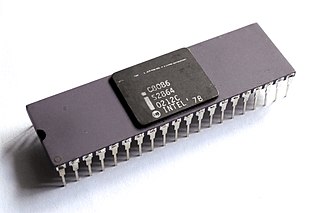
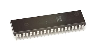
The 8085 is supplied in a 40-pin DIP package. To maximise the functions on the available pins, the 8085 uses a multiplexed address/data (AD0-AD7) bus. However, an 8085 circuit requires an 8-bit address latch, so Intel manufactured several support chips with an address latch built in. These include the 8755, with an address latch, 2 KB of EPROM and 16 I/O pins, and the 8155 with 256 bytes of RAM, 22 I/O pins and a 14-bit programmable timer/counter. The multiplexed address/data bus reduced the number of PCB tracks between the 8085 and such memory and I/O chips.
Both the 8080 and the 8085 were eclipsed by the Zilog Z80 for desktop computers, which took over most of the CP/M computer market, as well as a share of the booming home-computer market in the early-to-mid-1980s.
The 8085 had a long life as a controller, no doubt thanks to its built-in serial I/O and five prioritized interrupts, arguably microcontroller-like features that the Z80 CPU did not have. Once designed into such products as the DECtape II controller and the VT102 video terminal in the late 1970s, the 8085 served for new production throughout the lifetime of those products. This was typically longer than the product life of desktop computers.
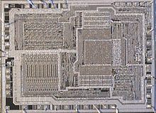
Intel 8085A CPU die
Description
i8085 microarchitecturei8085 pinout
The 8085 is a conventional von Neumann design based on the Intel 8080. Unlike the 8080 it does not multiplex state signals onto the data bus, but the 8-bit data bus is instead multiplexed with the lower eight bits of the 16-bit address bus to limit the number of pins to 40. State signals are provided by dedicated bus control signal pins and two dedicated bus state ID pins named S0 and S1. Pin 40 is used for the power supply (+5V) and pin 20 for ground. Pin 39 is used as the Hold pin.
The processor was designed using nMOS circuitry, and the later "H" versions were implemented in Intel's enhanced nMOS process called HMOS II ("High-performance MOS"), originally developed for fast static RAM products.[3] Only a single 5-volt power supply is needed, like competing processors and unlike the 8080. The 8085 uses approximately 6,500 transistors.[4]
The 8085 incorporates the functions of the 8224 (clock generator) and the 8228 (system controller) on chip, increasing the level of integration. A downside compared to similar contemporary designs (such as the Z80) is the fact that the buses require demultiplexing; however, address latches in the Intel 8155, 8355, and 8755 memory chips allow a direct interface, so an 8085 along with these chips is almost a complete system.
The 8085 has extensions to support new interrupts, with three maskable vectored interrupts (RST 7.5, RST 6.5 and RST 5.5), one non-maskable interrupt (TRAP), and one externally serviced interrupt (INTR). Each of these five interrupts has a separate pin on the processor, a feature which permits simple systems to avoid the cost of a separate interrupt controller. The RST 7.5 interrupt is edge triggered (latched), while RST 5.5 and 6.5 are level-sensitive. All interrupts except TRAP are enabled by the EI instruction and disabled by the DI instruction. In addition, the SIM (Set Interrupt Mask) and RIM (Read Interrupt Mask) instructions, the only instructions of the 8085 that are not from the 8080 design, allow each of the three maskable RST interrupts to be individually masked. All three are masked after a normal CPU reset. SIM and RIM also allow the global interrupt mask state and the three independent RST interrupt mask states to be read, the pending-interrupt states of those same three interrupts to be read, the RST 7.5 trigger-latch flip-flop to be reset (cancelling the pending interrupt without servicing it), and serial data to be sent and received via the SOD and SID pins, respectively, all under program control and independently of each other.
SIM and RIM each execute in four clock cycles (T states), making it possible to sample SID and/or toggle SOD considerably faster than it is possible to toggle or sample a signal via any I/O or memory-mapped port, e.g. one of the port of an 8155. (In this way, SID can be compared to the SO ["Set Overflow"] pin of the 6502 CPU contemporary to the 8085.)
Like the 8080, the 8085 can accommodate slower memories through externally generated wait states (pin 35, READY), and has provisions for Direct Memory Access (DMA) using HOLD and HLDA signals (pins 39 and 38). An improvement over the 8080 is that the 8085 can itself drive a piezoelectric crystal directly connected to it, and a built-in clock generator generates the internal high-amplitude two-phase clock signals at half the crystal frequency (a 6.14MHz crystal would yield a 3.07MHz clock, for instance). The internal clock is available on an output pin, to drive peripheral devices or other CPUs in lock-step synchrony with the CPU from which the signal is output. The 8085 can also be clocked by an external oscillator (making it feasible to use the 8085 in synchronous multi-processor systems using a system-wide common clock for all CPUs, or to synchronize the CPU to an external time reference such as that from a video source or a high-precision time reference).
The 8085 is a binary compatible follow-up on the 8080. It supports the complete instruction set of the 8080, with exactly the same instruction behavior, including all effects on the CPU flags (except for the AND/ANI operation, which sets the AC flag differently).[5] This means that the vast majority of object code (any program image in ROM or RAM) that runs successfully on the 8080 can run directly on the 8085 without translation or modification. (Exceptions include timing-critical code and code that is sensitive to the aforementioned difference in the AC flag setting or differences in undocumented CPU behavior.) 8085 instruction timings differ slightly from the 8080—some 8-bit operations, including INR, DCR, and the heavily used MOV r,r' instruction, are one clock cycle faster, but instructions that involve 16-bit operations, including stack operations (which increment or decrement the 16-bit SP register) generally one cycle slower. It is of course possible that the actual 8080 and/or 8085 differs from the published specifications, especially in subtle details. (The same is not true of the Z80.) As mentioned already, only the SIM and RIM instructions were new to the 8085.[nb 1]
The processor has seven 8-bit registers accessible to the programmer, named A, B, C, D, E, H, and L, where A is also known as the accumulator. The other six registers can be used as independent byte-registers or as three 16-bit register pairs, BC, DE, and HL (or B, D, H, as referred to in Intel documents), depending on the particular instruction.
Some instructions use HL as a (limited) 16-bit accumulator. As in the 8080, the contents of the memory address pointed to by HL can be accessed as pseudo register M. It also has a 16-bit program counter and a 16-bit stack pointer to memory (replacing the 8008's internal stack). Instructions such as PUSH PSW, POP PSW affect the Program Status Word (accumulator and flags). The accumulator stores the results of arithmetic and logical operations, and the flags register bits (sign, zero, auxiliary carry, parity, and carry flags) are set or cleared according to the results of these operations. The sign flag is set if the result has a negative sign (i.e. it is set if bit 7 of the accumulator is set). The auxiliary or half carry flag is set if a carryover from bit 3 to bit 4 occurred. The parity flag is set to 1 if the parity (number of 1-bits) of the accumulator is even; if odd, it is cleared. The zero flag is set if the result of the operation was 0. Lastly, the carry flag is set if a carryover from bit 7 of the accumulator (the MSB) occurred.
Commands/instructions
As in many other 8-bit processors, all instructions are encoded in a single byte (including register-numbers, but excluding immediate data), for simplicity. Some of them are followed by one or two bytes of data, which can be an immediate operand, a memory address, or a port number. A NOP "no operation" instruction exists, but does not modify any of the registers or flags. Like larger processors, it has CALL and RET instructions for multi-level procedure calls and returns (which can be conditionally executed, like jumps) and instructions to save and restore any 16-bit register-pair on the machine stack. There are also eight one-byte call instructions (RST) for subroutines located at the fixed addresses 00h, 08h, 10h,...,38h. These are intended to be supplied by external hardware in order to invoke a corresponding interrupt-service routine, but are also often employed as fast system calls. One sophisticated instruction is XTHL, which is used for exchanging the register pair HL with the value stored at the address indicated by the stack pointer.
8-bit instructions
All two-operand 8-bit arithmetic and logical (ALU) operations work on the 8-bit accumulator (the A register). For two-operand 8-bit operations, the other operand can be either an immediate value, another 8-bit register, or a memory cell addressed by the 16-bit register pair HL. The only 8-bit ALU operations that can have a destination other than the accumulator are the unary incrementation or decrementation instructions, which can operate on any 8-bit register or on memory addressed by HL, as for two-operand 8-bit operations. Direct copying is supported between any two 8-bit registers and between any 8-bit register and an HL-addressed memory cell, using the MOV instruction. An immediate value can also be moved into any of the foregoing destinations, using the MVI instruction. Due to the regular encoding of the MOV instruction (using nearly a quarter of the entire opcode space) there are redundant codes to copy a register into itself (MOV B,B, for instance), which are of little use, except for delays.[nb 2] However, what would have been a copy from the HL-addressed cell into itself (i.e., MOV M,M) instead encodes the HLT instruction, halting execution until an external reset or unmasked interrupt occurs.[nb 3]
16-bit operations
Although the 8085 is an 8-bit processor, it has some 16-bit operations. Any of the three 16-bit register pairs (BC, DE, HL) or SP can be loaded with an immediate 16-bit value (using LXI), incremented or decremented (using INX and DCX), or added to HL (using DAD). LHLD loads HL from directly addressed memory and SHLD stores HL likewise. The XCHG operation exchanges the values of HL and DE. XTHL exchanges last item pushed on stack with HL. Adding HL to itself performs a 16-bit arithmetic left shift with one instruction. The only 16-bit instruction that affects any flag is DAD (adding BC, DE, HL, or SP to HL), which updates the carry flag to facilitate 24-bit or larger additions and left shifts. Adding the stack pointer to HL is useful for indexing variables in (recursive) stack frames. A stack frame can be allocated using DAD SP and SPHL, and a branch to a computed pointer can be done with PCHL. These abilities make it feasible to compile languages such as PL/M, Pascal, or C with 16-bit variables and produce 8085 machine code. Subtraction and bitwise logical operations on 16 bits is done in 8-bit steps. Operations that have to be implemented by program code (subroutine libraries) include comparisons of signed integers as well as multiplication and division.
Undocumented instructions
A number of undocumented instructions and flags were discovered by two software engineers, Wolfgang Dehnhardt and Villy M. Sorensen in the process of developing an 8085 assembler. These instructions use 16-bit operands and include indirect loading and storing of a word, a subtraction, a shift, a rotate, and offset operations.[6]
By the time 8085 was designed but not yet announced, many designers found it to be inferior to the competing products already on the market. A next generation 8086 CPU was already in development. Intel made a last minute decision to leave 10 out of 12 new 8085 instructions undocumented to speed up and simplify the design of the upcoming 8086 CPU.[7]
Input/output scheme
The 8085 supports both port-mapped and memory-mapped I/O. It supports up to 256 input/output (I/O) ports via dedicated Input/Output instructions, with port addresses as operands. Port-mapped IO can be an advantage on processors with limited address space. During a port-mapped I/O bus cycle, the 8-bit I/O address is output by the CPU on both the lower and upper halves of the 16-bit address bus.
Devices designed for memory mapped I/O can also be accessed by using the LDA (load accumulator from a 16-bit address) and STA (store accumulator at a 16-bit address specified) instructions, or any other instructions that have memory operands. A memory-mapped IO transfer cycle appears on the bus as a normal memory access cycle.
Intel produced a series of development systems for the 8080 and 8085, known as the MDS-80 Microprocessor System. The original development system had an 8080 processor. Later 8085 and 8086 support was added including ICE (in-circuit emulators). It is a large and heavy desktop box, about a 20" cube (in the Intel corporate blue color) which includes a CPU, monitor, and a single 8-inch floppy disk drive. Later an external box was made available with two more floppy drives. It runs the ISIS operating system and can also operate an emulator pod and an external EPROM programmer. This unit uses the Multibus card cage which was intended just for the development system. A surprising number of spare card cages and processors were being sold, leading to the development of the Multibus as a separate product.
The later iPDS is a portable unit, about 8" × 16" × 20", with a handle. It has a small green screen, a keyboard built into the top, a 5¼ inch floppy disk drive, and runs the ISIS-II operating system. It can also accept a second 8085 processor, allowing a limited form of multi-processor operation where both processors run simultaneously and independently. The screen and keyboard can be switched between them, allowing programs to be assembled on one processor (large programs took a while) while files are edited in the other. It has a bubble memory option and various programming modules, including EPROM, and Intel 8048 and 8051 programming modules which are plugged into the side, replacing stand-alone device programmers. In addition to an 8080/8085 assembler, Intel produced a number of compilers including those for PL/M-80 and Pascal, and a set of tools for linking and statically locating programs to enable them to be burned into EPROMs and used in embedded systems.
A lower cost "MCS-85 System Design Kit" (SDK-85) board contains an 8085 CPU, an 8355 ROM containing a debugging monitor program, an 8155 RAM and 22 I/O ports, an 8279 hex keypad and 8-digit 7-segment LED, and a TTY (Teletype) 20mA current loop serial interface. Pads are available for one more 2K×8 8755 EPROM, and another 256byte RAM 8155 I/O Timer/Counter can be optionally added. All data, control, and address signals are available on dual pin headers, and a large prototyping area is provided.
The 8085 processor was used in a few early personal computers, for example, the TRS-80 Model 100 line used an OKI manufactured 80C85 (MSM80C85ARS). The CMOS version 80C85 of the NMOS/HMOS 8085 processor has several manufacturers. In the Soviet Union, an 80C85 clone was developed under the designation IM1821VM85A (Russian: ИМ1821ВМ85А[ru]) which in[update] 2016 was still in production.[11] Some manufacturers provide variants with additional functions such as additional instructions.[citation needed]
Pro-Log Corp. put the 8085 and supporting hardware on an STD Bus format card containing CPU, RAM, sockets for ROM/EPROM, I/O and external bus interfaces. The included Instruction Set Reference Card uses entirely different mnemonics for the Intel 8085 CPU. The product was a direct competitor to Intel's Multibus card offerings.
The 8085 CPU is one part of a family of chips developed by Intel for building a complete system. Many of these support chips were also used with other processors. The original IBM PC based on the Intel 8088 processor used several of these chips; the equivalent functions today are provided by VLSI chips, namely the "Southbridge" chips.
8155 – 2K-bit static MOS RAM with 3 I/O Ports and Timer. The industrial version of ID8155 was available for US$37.50 in quantities of 100 and up.[9][13] The military version of M8155 was available for US$100.00 in quantities of 100.[10] There is a 5MHz version of Intel 8155–2.[8] The available 8155H was introduced using the HMOS II technology which it uses 30 percent less power than the previous generation. The plastic package version of P8155H (3MHz) and P8155H-2 (5MHz) are available for US$5.15 and US$6.40 per 100 in quantities respectively.[3]
8156 – 2K-bit static MOS RAM with 3 I/O Ports and Timer. The industrial version of ID8156 was available for US$37.50 in quantities of 100.[9][13] There is a 5MHz version of Intel 8156–2.[8] The available 8156H was introduced using the HMOS II technology which it uses 30 percent less power than the previous generation. The plastic package version of P8156H (3MHz) and P8156H-2 (5MHz) are available for US$5.15 and US$6.40 per 100 in quantities respectively.[3]
8185 – 1,024 x 8-bit Static RAM. It included three chip selects and an internal address latch driven directly by the 8085's ALE. The 5MHz version of Intel 8185-2 was available for US$48.75 in quantity of 100.[8]
ROM memory
8355 – 2,048 × 8-bit ROM, two 8-bit I/O ports. The industrial version of ID8355 was available for US$22.00 in quantities of 1000.[9] There is a 5MHz version of Intel 8355–2.[8]
8755 – 2048 x 8-bit EPROM, two 8-bit I/O ports. The Intel 8755A-2 is the 5MHz version. That version was available for US$81.00 in quantity of 100.[8] There was an Industrial Grade version Intel I8755A-8.[13]
RAM controllers
8202 – Dynamic RAM Controller. This supports the Intel 2104A, 2117, or 2118 DRAM modules, up to 128 KB of DRAM modules. Price was reduced to US$36.25 for quantities of 100 for the D8202 package style around May 1979.[14]
8203 – Dynamic RAM Controller. The Intel 82C03 CMOS version dissipates less than 25 mA. It supports up to 16x 64K-bit RAM for a total capacity of up to 256KB. It refreshes every 10 to 16 microseconds. It supports multiplexing of row and column memory addresses. It generates strobes to latch the address internally. It arbitrates between simultaneous requests for memory access and refresh. It also acknowledges memory-access cycles to the system CPU. The 82C03 was available in either ceramic or plastic packages for US$32.00 in 100 pieces quantity.[15]
8207 – DRAM Controller
Periphery
8206 – Error Detection & Correction Unit
8210 – TTL To MOS Shifter & High Voltage Clock Driver
8212 – 8-bit I/O Port. The industrial version of ID8212 was available for US$6.75 in quantities of 100.[9]
8216 – 4-bit Parallel Bidirectional Bus Driver. The industrial version of ID8216 was available for US$6.40 in quantities of 100.[9]
8218/8219 – Bus Controller
8226 – 4-bit Parallel Bidirectional Bus Driver. The industrial version of ID8226 was available for US$6.40 in quantities of 100.[9]
8256 – Multifunction Peripheral. This multifunction chip uses Serial Communications, Parallel I/O, Counter/Timers and Interrupts. The Intel 8256AH was available for US$21.40 in quantities of 100.[17] This integrated circuit chip integrates the chips with the following functionality:
8273 – Programmable HDLC/SDLC Protocol Controller. This device supports ISO/CCITT's HDLC and IBM's SDLC communication protocols. These were available for US$33.75 (4MHz) and US$30.00 (8MHz) in quantities of 100.[18]
8274 – Multi-Protocol Serial Controller. This support three different protocols using the following feature of Asynchronous Operation, Byte Synchronous Operation and Bit Synchronous Operation. The Byte Synchronous mode is compatible to IBM's Bisync signal protocol. The Bit Synchronous mode is compatible to IBM's SDLC and the International Standards Organization's HDLC protocol and is compatible with CCITT X.25 international standard as well. It was packaged in 40-pin product using the Intel's HMOS technology. The available version is rated up to 880 kilobaud for US$30.30 in the quantities of 100.[19] NEC µPD7201 was also compatible.
8275 – Programmable CRT Controller. It refreshes the raster scan display by buffering from main memory and keeping track of the display portion. This version was available for US$32.00 in quantities of 100.[18]
8291 – GPIB Talker/Listener. This controller can operate from 1 to 8MHz. It was available for US$23.75 in quantities of 100.[18]
8292 – GPIB Controller. Designed around Intel 8041A which it has been programmed as an controller interface element. It also controls the bus using three lock-up timers to detect issues on the GPIB bus interface. It was available for US$21.25 in quantities of 100.[18]
8293 – GPIB Transceiver. This chipset supports up to 4 different modes: Mode 0 Talker/Listener Control Lines, Mode 1 Talker/Listener/Controller Control Lines, Mode 2 Talker/Listener/Controller Data Lines, and Mode 3 Talker/Listener Data Lines. It was available for US$11.50 in quantities of 100. At the time of release, it was available in samples then full production in the first quarter of 1980.[20]
8294 – Data Encryption/Decryption Unit + 1 O/P Port. It encrypts and decrypts 64-bit blocks of data using the Federal Information Processing Data Encryption Standard algorithm. This also uses the National Bureau of Standards encryption algorithm. This DEU operates using a 56-bit user-specified key to generate 64-bit cipher words. It was available for US$22.50 in quantities of 100.[18]
8295 – Dot Matrix Printer Controller. This interfaces with LRC 7040 Series dot matrix printers and other small printers as well. It was available for US$20.65 in quantities of 100.[18]
Educational use
In many engineering schools the 8085 processor is used in introductory microprocessor courses. Trainer kits composed of a printed circuit board, 8085, and supporting hardware are offered by various companies. These kits usually include complete documentation allowing a student to go from soldering to assembly language programming in a single course. Also, the architecture and instruction set of the 8085 are easy for a student to understand. Shared Project versions of educational and hobby 8085-based single-board computers are noted below in the External Links section of this article.
Simulators
Software simulators are available for the 8085 microprocessor, which allow simulated execution of opcodes in a graphical environment.
↑ Note that the Z80 assigns different instructions—two of the Z80's 6 relative jumps—to the opcodes that the 8085 uses for RIM and SIM, making 8085 programs that use these instructions generally unable to run on the Z80 without modification. Since use of these instructions usually relates to 8085-specific hardware features, the necessary program modification would typically be nontrivial.
↑ Even so, there is no need for seven different effectively identical delay instructions, and they are also identical in effect and form to the NOP instruction, except that NOP conveniently has the opcode 00 hex.
↑ (The TRAP interrupt, being an NMI, can always bring the 8085 out of the HALT state.)
Related Research Articles
The Intel 80286 is a 16-bit microprocessor that was introduced on February 1, 1982. It was the first 8086-based CPU with separate, non-multiplexed address and data buses and also the first with memory management and wide protection abilities. The 80286 used approximately 134,000 transistors in its original nMOS (HMOS) incarnation and, just like the contemporary 80186, it could correctly execute most software written for the earlier Intel 8086 and 8088 processors.
The Intel 8080 ("eighty-eighty") is the second 8-bit microprocessor designed and manufactured by Intel. It first appeared in April 1974 and is an extended and enhanced variant of the earlier 8008 design, although without binary compatibility. The initial specified clock rate or frequency limit was 2 MHz, with common instructions using 4, 5, 7, 10, or 11 cycles. As a result, the processor is able to execute several hundred thousand instructions per second. Two faster variants, the 8080A-1 and 8080A-2, became available later with clock frequency limits of 3.125 MHz and 2.63 MHz respectively. The 8080 needs two support chips to function in most applications: the i8224 clock generator/driver and the i8228 bus controller. It is implemented in N-type metal–oxide–semiconductor logic (NMOS) using non-saturated enhancement mode transistors as loads thus demanding a +12 V and a −5 V voltage in addition to the main transistor–transistor logic (TTL) compatible +5 V.
The 8086 is a 16-bit microprocessor chip designed by Intel between early 1976 and June 8, 1978, when it was released. The Intel 8088, released July 1, 1979, is a slightly modified chip with an external 8-bit data bus, and is notable as the processor used in the original IBM PC design.
The Intel 8088 microprocessor is a variant of the Intel 8086. Introduced on June 1, 1979, the 8088 has an eight-bit external data bus instead of the 16-bit bus of the 8086. The 16-bit registers and the one megabyte address range are unchanged, however. In fact, according to the Intel documentation, the 8086 and 8088 have the same execution unit (EU)—only the bus interface unit (BIU) is different. The 8088 was used in the original IBM PC and in IBM PC compatible clones.
The Intel 386, originally released as 80386 and later renamed i386, is a 32-bit microprocessor introduced in 1985. The first versions had 275,000 transistors and were the central processing unit (CPU) of many workstations and high-end personal computers of the time.
The Intel 80186, also known as the iAPX 186, or just 186, is a microprocessor and microcontroller introduced in 1982. It was based on the Intel 8086 and, like it, had a 16-bit external data bus multiplexed with a 20-bit address bus.
The Motorola 6809 ("sixty-eight-oh-nine") is an 8-bit microprocessor with some 16-bit features. It was designed by Motorola's Terry Ritter and Joel Boney and introduced in 1978. Although source compatible with the earlier Motorola 6800, the 6809 offered significant improvements over it and 8-bit contemporaries like the MOS Technology 6502, including a hardware multiplication instruction, 16-bit arithmetic, system and user stack registers allowing re-entrant code, improved interrupts, position-independent code and an orthogonal instruction set architecture with a comprehensive set of addressing modes.
The Z80 is an 8-bit microprocessor introduced by Zilog as the startup company's first product. The Z80 was conceived by Federico Faggin in late 1974 and developed by him and his 11 employees starting in early 1975. The first working samples were delivered in March 1976, and it was officially introduced on the market in July 1976. With the revenue from the Z80, the company built its own chip factories and grew to over a thousand employees over the following two years.
The NS32000, sometimes known as the 32k, is a series of microprocessors produced by National Semiconductor. The first member of the family came to market in 1982, briefly known as the 16032 before becoming the 32016. It was the first general-purpose microprocessor on the market that used 32-bit data throughout: the Motorola 68000 used 32-bit data but had a 16-bit ALU and thus took twice as long perform many operations. However, the 32016 contained many bugs and often could not be run at its rated speed. These problems, and the presence of the otherwise similar 68000 which had been available since 1980, led to little use in the market.
The Intel 8008 is an early 8-bit microprocessor capable of addressing 16 KB of memory, introduced in April 1972. The 8008 architecture was designed by Computer Terminal Corporation (CTC) and was implemented and manufactured by Intel. While the 8008 was originally designed for use in CTC's Datapoint 2200 programmable terminal, an agreement between CTC and Intel permitted Intel to market the chip to other customers after Seiko expressed an interest in using it for a calculator.
Intel's i960 was a RISC-based microprocessor design that became popular during the early 1990s as an embedded microcontroller. It became a best-selling CPU in that segment, along with the competing AMD 29000. In spite of its success, Intel stopped marketing the i960 in the late 1990s, as a result of a settlement with DEC whereby Intel received the rights to produce the StrongARM CPU. The processor continues to be used for a few military applications.
The Fairchild F8 is an 8-bit microprocessor system from Fairchild Semiconductor, announced in 1974 and shipped in 1975. The original processor family included four main 40-pin integrated circuits (ICs); the 3850 CPU which was the arithmetic logic unit, the 3851 Program Storage Unit (PSU) which contained 1 KB of program ROM and handled instruction decoding, and the optional 3852 Dynamic Memory Interface (DMI) or 3853 Static Memory Interface (SMI) to control additional RAM or ROM holding the user programs or data. The 3854 DMA was another optional system that added direct memory access into the RAM controlled by the 3852.
National Semiconductor's SC/MP for Simple Cost-effective Micro Processor, is an early 8-bit microprocessor which became available in April 1976. It was designed to allow systems to be implemented with the minimum number of additional support chips. SC/MP included a daisy-chained control pin that allowed up to three SC/MP's share a single main memory to produce a multiprocessor system, or to act as controllers in a system with another main central processing unit (CPU). Three versions were released over its lifetime, SCMP-1 through 3, the latter two also known as INS8060 and INS8070.
The Intel 8259 is a programmable interrupt controller (PIC) designed for the Intel 8085 and Intel 8086 microprocessors. The initial part was 8259, a later A suffix version was upward compatible and usable with the 8086 or 8088 processor. The 8259 combines multiple interrupt input sources into a single interrupt output to the host microprocessor, extending the interrupt levels available in a system beyond the one or two levels found on the processor chip. The 8259A was the interrupt controller for the ISA bus in the original IBM PC and IBM PC AT.
The Signetics 2650 was an 8-bit microprocessor introduced in July 1975. According to Adam Osborne's book An Introduction to Microprocessors Vol 2: Some Real Products, it was "the most minicomputer-like" of the microprocessors available at the time. A combination of missing features and odd memory access limited its appeal, and the system saw little use in the market.
The Intel 8255 Programmable Peripheral Interface (PPI) chip was developed and manufactured by Intel in the first half of the 1970s for the Intel 8080 microprocessor. The 8255 provides 24 parallel input/output lines with a variety of programmable operating modes.
The KR580VM80A is a Soviet microprocessor, a clone of the Intel 8080 CPU. Different versions of this CPU were manufactured beginning in the late 1970s, the earliest known use being in the SM1800 computer in 1979. Initially called the K580IK80 (К580ИК80), it was produced in a 48-pin planar metal-ceramic package. Later, a version in a PDIP-40 package was produced and was named the KR580IK80A (КР580ИК80А). The pin layout of the latter completely matched that of Intel's 8080A CPU. In 1986 this CPU received a new part number to conform with the 1980 Soviet integrated circuit designation and became known as the KR580VM80A (КР580ВМ80А), the number it is most widely known by today. Normal clock frequency for the K580IK80A is 2 MHz, with speeds up to 2.5 MHz for the KR580VM80A. The KR580IK80A was manufactured in a 6 µm process. In the later KR580VM80A the feature size was reduced to 5 µm and the die became 20% smaller.
The CP1600 is a 16-bit microprocessor created in a partnership between General Instrument and Honeywell, introduced in February 1975. It is one of the first single-chip 16-bit processors. The overall design bears a strong resemblance to the PDP-11.
The NEC μCOM series is a series of microprocessors and microcontrollers manufactured by NEC in the 1970s and 1980s. The initial entries in the series were custom-designed 4 and 16-bit designs, but later models in the series were mostly based on the Intel 8080 and Zilog Z80 8-bit designs, and later, the Intel 8086 16-bit design. Most of the line was replaced in 1984 by the NEC V20, an Intel 8088 clone.
↑ Mazor, Stanley (January–March 2010). "Intel's 8086". IEEE Annals of the History of Computing. IEEE Computer Society: 75–79. ISSN1058-6180.
1 2 3 4 5 6 Intel Corporation, "New EPROM completes 5MHz capability for MCS-85™ family", Intel Preview, January/February 1980, p. 24.
1 2 3 4 5 6 7 Intel Corporation, "Microcomputer Component: New industrial grade product line answers the demand for high-reliability components to operate in industrial applications.", Intel Preview, March/April 1979, p. 11.
1 2 3 Intel Corporation, "8086 Available for industrial environment", Intel Preview Special Issue: 16-Bit Solutions, May/June 1980, p. 29.
↑ Intel Corporation, "Microcomputer Components: Intel reduces prices on the 8202, the first single chip, complete solution to dynamic RAM control", Intel Preview, May/June 1979, p. 11.
↑ Intel Corporation, "New Product Focus Components: A Refreshing New Dynamic RAM Controller", Solutions, July/August 1984, Page 12.
↑ Intel Corporation, "NewsBit: Intel Licenses Oki on CMOS Version of Several Products", Solutions, July/August 1984, Page 1.
↑ Intel Corporation, "New Product Focus Components: Peripheral Vision: The 8256AH Combines Four Chips In One", Solutions, July/August 1984, Page 13.
1 2 3 4 5 6 7 Intel Corporation, "Intel peripherals enhance 8086 system design", Intel Preview Special Issue: 16-Bit Solution, May/June 1980, p. 22.
↑ Intel Corporation, "New Products: High-Speed Controller Supports Three Protocols", Solutions, July/August 1981, Page 18
Gaonkar, Ramesh (December 2000). Microprocessor Architecture, Programming and Applications with the 8085. Penram International Publishing. ISBN81-87972-09-2.
Bill Detwiler Tandy TRS-80 Model 100 Teardown Tech Republic, 2011 Web
This page is based on this Wikipedia article Text is available under the CC BY-SA 4.0 license; additional terms may apply. Images, videos and audio are available under their respective licenses.