
Pentium is a discontinued series of x86 architecture-compatible microprocessors produced by Intel. The original Pentium was first released on March 22, 1993. The name "Pentium" is originally derived from the Greek word pente (πεντε), meaning "five", a reference to the prior numeric naming convention of Intel's 80x86 processors (8086–80486), with the Latin ending -ium since the processor would otherwise have been named 80586 using that convention.
The "22 nm" node is the process step following 32 nm in CMOS MOSFET semiconductor device fabrication. The typical half-pitch for a memory cell using the process is around 22 nm. It was first demonstrated by semiconductor companies for use in RAM memory in 2008. In 2010, Toshiba began shipping 24 nm flash memory chips, and Samsung Electronics began mass-producing 20 nm flash memory chips. The first consumer-level CPU deliveries using a 22 nm process started in April 2012 with the Intel Ivy Bridge processors.
The "14 nanometer process" refers to a marketing term for the MOSFET technology node that is the successor to the "22 nm" node. The "14 nm" was so named by the International Technology Roadmap for Semiconductors (ITRS). Until about 2011, the node following "22 nm" was expected to be "16 nm". All "14 nm" nodes use FinFET technology, a type of multi-gate MOSFET technology that is a non-planar evolution of planar silicon CMOS technology.
Tick–tock was a production model adopted in 2007 by chip manufacturer Intel. Under this model, every microarchitecture change (tock) was followed by a die shrink of the process technology (tick). It was replaced by the process–architecture–optimization model, which was announced in 2016 and is like a tick–tock cycle followed by an optimization phase. As a general engineering model, tick–tock is a model that refreshes one side of a binary system each release cycle.

Intel Core is a line of multi-core central processing units (CPUs) for midrange, embedded, workstation, high-end and enthusiast computer markets marketed by Intel Corporation. These processors displaced the existing mid- to high-end Pentium processors at the time of their introduction, moving the Pentium to the entry level. Identical or more capable versions of Core processors are also sold as Xeon processors for the server and workstation markets.

Intel Graphics Technology (GT) is the collective name for a series of integrated graphics processors (IGPs) produced by Intel that are manufactured on the same package or die as the central processing unit (CPU). It was first introduced in 2010 as Intel HD Graphics and renamed in 2017 as Intel UHD Graphics.

Skylake is Intel's codename for its sixth generation Core microprocessor family that was launched on August 5, 2015, succeeding the Broadwell microarchitecture. Skylake is a microarchitecture redesign using the same 14 nm manufacturing process technology as its predecessor, serving as a tock in Intel's tick–tock manufacturing and design model. According to Intel, the redesign brings greater CPU and GPU performance and reduced power consumption. Skylake CPUs share their microarchitecture with Kaby Lake, Coffee Lake, Whiskey Lake, and Comet Lake CPUs.
Intel Quick Sync Video is Intel's brand for its dedicated video encoding and decoding hardware core. Quick Sync was introduced with the Sandy Bridge CPU microarchitecture on 9 January 2011 and has been found on the die of Intel CPUs ever since.

Broadwell is the fifth generation of the Intel Core processor. It is Intel's codename for the 14 nanometer die shrink of its Haswell microarchitecture. It is a "tick" in Intel's tick–tock principle as the next step in semiconductor fabrication. Like some of the previous tick-tock iterations, Broadwell did not completely replace the full range of CPUs from the previous microarchitecture (Haswell), as there were no low-end desktop CPUs based on Broadwell.
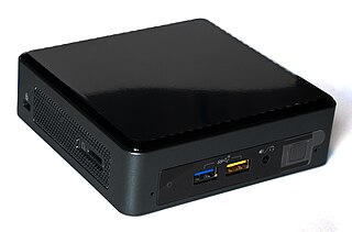
Next Unit of Computing (NUC) is a line of small-form-factor barebone computer kits designed by Intel. It was previewed in 2012 and launched in early 2013. The NUC has developed over ten generations, spanning from Sandy Bridge-based Celeron CPUs in the first generation through Ivy Bridge-based Core i3 and i5 CPUs in the second generation to Gemini Lake-based Pentium and Celeron CPUs and Kaby Lake-based Core i3, i5, and i7 CPUs in the seventh and eighth generations. The NUC motherboard usually measures approximately 10 × 10 centimetres (4 × 4 in), although some models have had different dimensions.

Kaby Lake is Intel's codename for its seventh generation Core microprocessor family announced on August 30, 2016. Like the preceding Skylake, Kaby Lake is produced using a 14 nanometer manufacturing process technology. Breaking with Intel's previous "tick–tock" manufacturing and design model, Kaby Lake represents the optimized step of the newer process–architecture–optimization model. Kaby Lake began shipping to manufacturers and OEMs in the second quarter of 2016, with its desktop chips officially launched in January 2017.
Ice Lake is Intel's codename for the 10th generation Intel Core mobile and 3rd generation Xeon Scalable server processors based on the Sunny Cove microarchitecture. Ice Lake represents an Architecture step in Intel's process–architecture–optimization model. Produced on the second generation of Intel's 10 nm process, 10 nm+, Ice Lake is Intel's second microarchitecture to be manufactured on the 10 nm process, following the limited launch of Cannon Lake in 2018. However, Intel altered their naming scheme in 2020 for the 10 nm process. In this new naming scheme, Ice Lake's manufacturing process is called simply 10 nm, without any appended pluses.
Tiger Lake is Intel's codename for the 11th generation Intel Core mobile processors based on the Willow Cove Core microarchitecture, manufactured using Intel's third-generation 10 nm process node known as 10SF. Tiger Lake replaces the Ice Lake family of mobile processors, representing an optimization step in Intel's process–architecture–optimization model.
Coffee Lake is Intel's codename for its eighth-generation Core microprocessor family, announced on September 25, 2017. It is manufactured using Intel's second 14 nm process node refinement. Desktop Coffee Lake processors introduced i5 and i7 CPUs featuring six cores and Core i3 CPUs with four cores and no hyperthreading.

Ryzen is a brand of multi-core x86-64 microprocessors designed and marketed by Advanced Micro Devices (AMD) for desktop, mobile, server, and embedded platforms based on the Zen microarchitecture. It consists of central processing units (CPUs) marketed for mainstream, enthusiast, server, and workstation segments and accelerated processing units (APUs) marketed for mainstream and entry-level segments and embedded systems applications.
Process–architecture–optimization is a development model for central processing units (CPUs) that Intel adopted in 2016. Under this three-phase (three-year) model, every microprocessor die shrink is followed by a microarchitecture change and then by one or more optimizations. It replaced the two-phase (two-year) tick–tock model that Intel adopted in 2006. The tick–tock model was no longer economically sustainable, according to Intel, because production of ever smaller dies becomes ever more costly.
Sunny Cove is a codename for a CPU microarchitecture developed by Intel, first released in September 2019. It succeeds the Palm Cove microarchitecture and is fabricated using Intel's 10 nm process node. The microarchitecture is implemented in 10th-generation Intel Core processors for mobile and third generation Xeon scalable server processors. 10th-generation Intel Core mobile processors were released in September 2019, while the Xeon server processors were released on April 6, 2021.

Alder Lake is Intel's codename for the 12th generation of Intel Core processors based on a hybrid architecture utilizing Golden Cove performance cores and Gracemont efficient cores. It is fabricated using Intel's Intel 7 process, previously referred to as Intel 10 nm Enhanced SuperFin (10ESF). The 10ESF has a 10%-15% boost in performance over the 10SF used in the mobile Tiger Lake processors. Intel officially announced 12th Gen Intel Core CPUs on October 27, 2021, mobile CPUs and non-K series desktop CPUs on January 4, 2022, Alder Lake-P and -U series on February 23, 2022, and Alder Lake-HX series on May 10, 2022.
Willow Cove is a codename for a CPU microarchitecture developed by Intel and released in September 2020. Willow Cove is the successor to the Sunny Cove microarchitecture, and is fabricated using Intel's enhanced 10 nm process node called 10 nm SuperFin (10SF). The microarchitecture powers 11th-generation Intel Core mobile processors.
