Related Research Articles
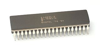
x86 is a family of complex instruction set computer (CISC) instruction set architectures initially developed by Intel based on the Intel 8086 microprocessor and its 8088 variant. The 8086 was introduced in 1978 as a fully 16-bit extension of Intel's 8-bit 8080 microprocessor, with memory segmentation as a solution for addressing more memory than can be covered by a plain 16-bit address. The term "x86" came into being because the names of several successors to Intel's 8086 processor end in "86", including the 80186, 80286, 80386 and 80486 processors.
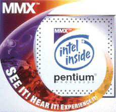
MMX is a single instruction, multiple data (SIMD) instruction set architecture designed by Intel, introduced on January 8, 1997 with its Pentium P5 (microarchitecture) based line of microprocessors, named "Pentium with MMX Technology". It developed out of a similar unit introduced on the Intel i860, and earlier the Intel i750 video pixel processor. MMX is a processor supplementary capability that is supported on IA-32 processors by Intel and other vendors as of 1997.
In computing, Streaming SIMD Extensions (SSE) is a single instruction, multiple data (SIMD) instruction set extension to the x86 architecture, designed by Intel and introduced in 1999 in their Pentium III series of Central processing units (CPUs) shortly after the appearance of Advanced Micro Devices (AMD's) 3DNow!. SSE contains 70 new instructions, most of which work on single precision floating-point data. SIMD instructions can greatly increase performance when exactly the same operations are to be performed on multiple data objects. Typical applications are digital signal processing and graphics processing.
3DNow! is a deprecated extension to the x86 instruction set developed by Advanced Micro Devices (AMD). It adds single instruction multiple data (SIMD) instructions to the base x86 instruction set, enabling it to perform vector processing of floating-point vector operations using vector registers, which improves the performance of many graphics-intensive applications. The first microprocessor to implement 3DNow! was the AMD K6-2, which was introduced in 1998. When the application was appropriate, this raised the speed by about 2–4 times.
SSE2 is one of the Intel SIMD processor supplementary instruction sets first introduced by Intel with the initial version of the Pentium 4 in 2000. It extends the earlier SSE instruction set, and is intended to fully replace MMX. Intel extended SSE2 to create SSE3 in 2004. SSE2 added 144 new instructions to SSE, which has 70 instructions. Competing chip-maker AMD added support for SSE2 with the introduction of their Opteron and Athlon 64 ranges of AMD64 64-bit CPUs in 2003.
SSE3, Streaming SIMD Extensions 3, also known by its Intel code name Prescott New Instructions (PNI), is the third iteration of the SSE instruction set for the IA-32 (x86) architecture. Intel introduced SSE3 in early 2004 with the Prescott revision of their Pentium 4 CPU. In April 2005, AMD introduced a subset of SSE3 in revision E of their Athlon 64 CPUs. The earlier SIMD instruction sets on the x86 platform, from oldest to newest, are MMX, 3DNow!, SSE, and SSE2.
The x86 instruction set refers to the set of instructions that x86-compatible microprocessors support. The instructions are usually part of an executable program, often stored as a computer file and executed on the processor.
Pentium is a series of x86 architecture-compatible microprocessors produced by Intel. The original Pentium was first released on March 22, 1993.
SSE4 is a SIMD CPU instruction set used in the Intel Core microarchitecture and AMD K10 (K8L). It was announced on September 27, 2006, at the Fall 2006 Intel Developer Forum, with vague details in a white paper; more precise details of 47 instructions became available at the Spring 2007 Intel Developer Forum in Beijing, in the presentation. SSE4 is fully compatible with software written for previous generations of Intel 64 and IA-32 architecture microprocessors. All existing software continues to run correctly without modification on microprocessors that incorporate SSE4, as well as in the presence of existing and new applications that incorporate SSE4.

The VIA Nano is a 64-bit CPU for personal computers. The VIA Nano was released by VIA Technologies in 2008 after five years of development by its CPU division, Centaur Technology. This new Isaiah 64-bit architecture was designed from scratch, unveiled on 24 January 2008, and launched on 29 May, including low-voltage variants and the Nano brand name. The processor supports a number of VIA-specific x86 extensions designed to boost efficiency in low-power appliances.
The SSE5 was a SIMD instruction set extension proposed by AMD on August 30, 2007 as a supplement to the 128-bit SSE core instructions in the AMD64 architecture.
Advanced Vector Extensions (AVX) are extensions to the x86 instruction set architecture for microprocessors from Intel and Advanced Micro Devices (AMD). They were proposed by Intel in March 2008 and first supported by Intel with the Sandy Bridge processor shipping in Q1 2011 and later by AMD with the Bulldozer processor shipping in Q3 2011. AVX provides new features, new instructions and a new coding scheme.
The XOP instruction set, announced by AMD on May 1, 2009, is an extension to the 128-bit SSE core instructions in the x86 and AMD64 instruction set for the Bulldozer processor core, which was released on October 12, 2011. However AMD removed support for XOP from Zen (microarchitecture) onward.
The VEX prefix and VEX coding scheme are an extension to the x86 and x86-64 instruction set architecture for microprocessors from Intel, AMD and others.
AVX-512 are 512-bit extensions to the 256-bit Advanced Vector Extensions SIMD instructions for x86 instruction set architecture (ISA) proposed by Intel in July 2013, and implemented in Intel's Xeon Phi x200 and Skylake-X CPUs; this includes the Core-X series, as well as the new Xeon Scalable Processor Family and Xeon D-2100 Embedded Series. AVX-512 consists of multiple extensions that may be implemented independently. This policy is a departure from the historical requirement of implementing the entire instruction block. Only the core extension AVX-512F is required by all AVX-512 implementations.
References
- 1 2 "2.9.5". Intel 64 and IA-32 Architectures Optimization Reference Manual (PDF) (Technical report). Intel.com. 2016. pp. 92–93. Archived (PDF) from the original on June 20, 2018. Retrieved June 22, 2018.