Streaming SIMD Extensions

Last updated

In computing, Streaming SIMD Extensions (SSE) is a single instruction, multiple data (SIMD) instruction set extension to the x86 architecture, designed by Intel and introduced in 1999 in their Pentium III series of central processing units (CPUs) shortly after the appearance of Advanced Micro Devices (AMD's) 3DNow!. SSE contains 70 new instructions (65 unique mnemonics [1] using 70 encodings), most of which work on single precision floating-point data. SIMD instructions can greatly increase performance when exactly the same operations are to be performed on multiple data objects. Typical applications are digital signal processing and graphics processing.

Contents

Intel's first IA-32 SIMD effort was the MMX instruction set. MMX had two main problems: it re-used existing x87 floating-point registers making the CPUs unable to work on both floating-point and SIMD data at the same time, and it only worked on integers. SSE floating-point instructions operate on a new independent register set, the XMM registers, and adds a few integer instructions that work on MMX registers.

SSE was subsequently expanded by Intel to SSE2, SSE3, SSSE3 and SSE4. Because it supports floating-point math, it had wider applications than MMX and became more popular. The addition of integer support in SSE2 made MMX largely redundant, though further performance increases can be attained in some situations[ when? ] by using MMX in parallel with SSE operations.

SSE was originally called Katmai New Instructions (KNI), Katmai being the code name for the first Pentium III core revision. During the Katmai project Intel sought to distinguish it from their earlier product line, particularly their flagship Pentium II. It was later renamed Internet Streaming SIMD Extensions (ISSE [2] ), then SSE.

AMD added a subset of SSE, 19 of them, called new MMX instructions, [3] and known as several variants and combinations of SSE and MMX, shortly after with the release of the original Athlon in August 1999, see 3DNow! extensions. AMD eventually added full support for SSE instructions, starting with its Athlon XP and Duron (Morgan core) processors.

Registers

SSE originally added eight new 128-bit registers known as XMM0 through XMM7. The AMD64 extensions from AMD (originally called x86-64) added a further eight registers XMM8 through XMM15, and this extension is duplicated in the Intel 64 architecture. There is also a new 32-bit control/status register, MXCSR. The registers XMM8 through XMM15 are accessible only in 64-bit operating mode.

XMM registers.svg

SSE used only a single data type for XMM registers:

SSE2 would later expand the usage of the XMM registers to include:

Because these 128-bit registers are additional machine states that the operating system must preserve across task switches, they are disabled by default until the operating system explicitly enables them. This means that the OS must know how to use the FXSAVE and FXRSTOR instructions, which is the extended pair of instructions that can save all x86 and SSE register states at once. This support was quickly added to all major IA-32 operating systems.

The first CPU to support SSE, the Pentium III, shared execution resources between SSE and the floating-point unit (FPU). [2] While a compiled application can interleave FPU and SSE instructions side-by-side, the Pentium III will not issue an FPU and an SSE instruction in the same clock cycle. This limitation reduces the effectiveness of pipelining, but the separate XMM registers do allow SIMD and scalar floating-point operations to be mixed without the performance hit from explicit MMX/floating-point mode switching.

SSE instructions

SSE introduced both scalar and packed floating-point instructions.

Floating-point instructions

Integer instructions

Other instructions

Example

The following simple example demonstrates the advantage of using SSE. Consider an operation like vector addition, which is used very often in computer graphics applications. To add two single precision, four-component vectors together using x86 requires four floating-point addition instructions.

vec_res.x=v1.x+v2.x;vec_res.y=v1.y+v2.y;vec_res.z=v1.z+v2.z;vec_res.w=v1.w+v2.w;

This corresponds to four x86 FADD instructions in the object code. On the other hand, as the following pseudo-code shows, a single 128-bit 'packed-add' instruction can replace the four scalar addition instructions.

movapsxmm0,[v1];xmm0 = v1.w | v1.z | v1.y | v1.x addpsxmm0,[v2];xmm0 = v1.w+v2.w | v1.z+v2.z | v1.y+v2.y | v1.x+v2.xmovaps[vec_res],xmm0;xmm0

Later versions

Identifying

The following programs can be used to determine which, if any, versions of SSE are supported on a system

Related Research Articles

x86 Family of instruction set architectures

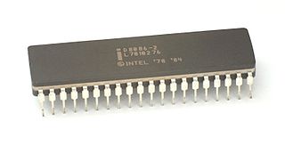
x86 is a family of complex instruction set computer (CISC) instruction set architectures initially developed by Intel based on the Intel 8086 microprocessor and its 8088 variant. The 8086 was introduced in 1978 as a fully 16-bit extension of Intel's 8-bit 8080 microprocessor, with memory segmentation as a solution for addressing more memory than can be covered by a plain 16-bit address. The term "x86" came into being because the names of several successors to Intel's 8086 processor end in "86", including the 80186, 80286, 80386 and 80486 processors. Colloquially, their names were "186", "286", "386" and "486".

<span class="mw-page-title-main">Single instruction, multiple data</span> Type of parallel processing

Single instruction, multiple data (SIMD) is a type of parallel processing in Flynn's taxonomy. SIMD can be internal and it can be directly accessible through an instruction set architecture (ISA), but it should not be confused with an ISA. SIMD describes computers with multiple processing elements that perform the same operation on multiple data points simultaneously.

<span class="mw-page-title-main">MMX (instruction set)</span> Instruction set designed by Intel

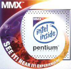
MMX is a single instruction, multiple data (SIMD) instruction set architecture designed by Intel, introduced on January 8, 1997 with its Pentium P5 (microarchitecture) based line of microprocessors, named "Pentium with MMX Technology". It developed out of a similar unit introduced on the Intel i860, and earlier the Intel i750 video pixel processor. MMX is a processor supplementary capability that is supported on IA-32 processors by Intel and other vendors as of 1997. AMD also added MMX instruction set in its K6 processor.

Visual Instruction Set, or VIS, is a SIMD instruction set extension for SPARC V9 microprocessors developed by Sun Microsystems. There are five versions of VIS: VIS 1, VIS 2, VIS 2+, VIS 3 and VIS 4.

3DNow! is a deprecated extension to the x86 instruction set developed by Advanced Micro Devices (AMD). It adds single instruction multiple data (SIMD) instructions to the base x86 instruction set, enabling it to perform vector processing of floating-point vector operations using vector registers. This improvement enhances the performance of many graphics-intensive applications. The first microprocessor to implement 3DNow! was the AMD K6-2, introduced in 1998. In appropriate applications, this enhancement raised the speed by about 2–4 times.

SSE2 is one of the Intel SIMD processor supplementary instruction sets introduced by Intel with the initial version of the Pentium 4 in 2000. SSE2 instructions allow the use of XMM (SIMD) registers on x86 instruction set architecture processors. These registers can load up to 128 bits of data and perform instructions, such as vector addition and multiplication, simultaneously.

SSE3, Streaming SIMD Extensions 3, also known by its Intel code name Prescott New Instructions (PNI), is the third iteration of the SSE instruction set for the IA-32 (x86) architecture. Intel introduced SSE3 in early 2004 with the Prescott revision of their Pentium 4 CPU. In April 2005, AMD introduced a subset of SSE3 in revision E of their Athlon 64 CPUs. The earlier SIMD instruction sets on the x86 platform, from oldest to newest, are MMX, 3DNow!, SSE, and SSE2.

The x86 instruction set refers to the set of instructions that x86-compatible microprocessors support. The instructions are usually part of an executable program, often stored as a computer file and executed on the processor.

<span class="mw-page-title-main">Athlon 64 X2</span> Series of CPUs by AMD

The Athlon 64 X2 is the first native dual-core desktop central processing unit (CPU) designed by Advanced Micro Devices (AMD). It was designed from scratch as native dual-core by using an already multi-CPU enabled Athlon 64, joining it with another functional core on one die, and connecting both via a shared dual-channel memory controller/north bridge and additional control logic. The initial versions are based on the E stepping model of the Athlon 64 and, depending on the model, have either 512 or 1024 KB of L2 cache per core. The Athlon 64 X2 can decode instructions for Streaming SIMD Extensions 3 (SSE3), except those few specific to Intel's architecture. The first Athlon 64 X2 CPUs were released in May 2005, in the same month as Intel's first dual-core processor, the Pentium D.

The AMD Family 10h, or K10, is a microprocessor microarchitecture by AMD based on the K8 microarchitecture. The first third-generation Opteron products for servers were launched on September 10, 2007, with the Phenom processors for desktops following and launching on November 11, 2007 as the immediate successors to the K8 series of processors.

Supplemental Streaming SIMD Extensions 3 is a SIMD instruction set created by Intel and is the fourth iteration of the SSE technology.

Advanced Vector Extensions are SIMD extensions to the x86 instruction set architecture for microprocessors from Intel and Advanced Micro Devices (AMD). They were proposed by Intel in March 2008 and first supported by Intel with the Sandy Bridge processor shipping in Q1 2011 and later by AMD with the Bulldozer processor shipping in Q3 2011. AVX provides new features, new instructions, and a new coding scheme.

Open Watcom Assembler or WASM is an x86 assembler produced by Watcom, based on the Watcom Assembler found in Watcom C/C++ compiler and Watcom FORTRAN 77. Further development is being done on the 32- and 64-bit JWASM project, which more closely matches the syntax of Microsoft's assembler.

References

  1. "Intel® 64 and IA-32 Architectures Software Developer's Manual Volume 1: Basic Architecture". Intel. April 2022. pp. 5-16–5-19. Archived from the original on April 25, 2022. Retrieved May 16, 2022.
  2. 1 2 Diefendorff, Keith (March 8, 1999). "Pentium III = Pentium II + SSE: Internet SSE Architecture Boosts Multimedia Performance" (PDF). Microprocessor Report . 13 (3). Archived (PDF) from the original on April 17, 2018. Retrieved September 1, 2017.
  3. "AMD Extensions to the 3DNow and MMX Instruction Sets Manual" (PDF). Advanced Micro Devices, Inc. March 2000. Archived from the original (PDF) on May 17, 2008. Retrieved April 18, 2024.
  4. Vance, Ashlee (August 3, 2007). "AMD plots single thread boost with x86 extensions". The Register . Archived from the original on April 27, 2011. Retrieved August 24, 2017.
  5. "AMD64 Technology: 128-Bit SSE5 Instruction Set" (PDF). AMD. August 2007. Archived (PDF) from the original on August 25, 2017. Retrieved August 24, 2017.
  6. "AMD64 Technology AMD64 Architecture Programmer's Manual Volume 6: 128-Bit and 256-Bit XOP and FMA4 Instructions" (PDF). AMD. November 2009. Archived (PDF) from the original on January 31, 2017. Retrieved August 24, 2017.
  7. Girkar, Milind (October 1, 2013). "Intel® Advanced Vector Extensions (Intel® AVX)". Intel. Archived from the original on August 25, 2017. Retrieved August 24, 2017.
  8. "Download the Intel® Processor Identification Utility". Intel. July 24, 2017. Archived from the original on August 25, 2017. Retrieved August 24, 2017.