General information | |
---|---|
Launched | December 14, 2023 [1] |
Marketed by | Intel |
Designed by | Intel |
Common manufacturer(s) | |
CPUID code | A06A4h |
Product code | 80723 [2] |
Performance | |
Max. CPU clock rate | P-cores: 5.1 GHz E-cores: 3.8 GHz LP E-cores: 2.5 GHz |
DMI speeds | x8 16 GT/s |
Cache | |
L1 cache | 112 KB per P-core:
96 KB per E-core and LP E-core:
|
L2 cache | 2 MB per P-core, E-core cluster and LP E-core cluster |
L3 cache | Up to 24 MB |
Architecture and classification | |
Application | Mobile |
Technology node | Intel 4 [3] TSMC N5 TSMC N6 Intel 22FFL |
Microarchitecture | Redwood Cove (P-cores) Crestmont (E-cores and LP E-cores) |
Instruction set | x86-64 |
Instructions | x86-64 |
Extensions | |
Physical specifications | |
Cores |
|
Memory (RAM) | |
GPU(s) | Intel Arc |
Package(s) |
|
Socket(s) |
|
Products, models, variants | |
Product code name(s) |
|
Model(s) |
|
Brand name(s) | |
History | |
Predecessor(s) | Alder Lake (embedded) Raptor Lake (9 W - 45 W premium mobile) |
Successor(s) | Arrow Lake(Desktop) Lunar Lake(Mobile) |
Support status | |
Supported |
Meteor Lake is Intel's codename for the first generation of Intel Core Ultra mobile processors, [4] and was officially launched on December 14, 2023. [5] It is the first generation of Intel mobile processors to use a chiplet architecture which means that the processor is a multi-chip module. [4] Tim Wilson led the system on a chip development for this generation microprocessor. [6]
In July 2021, Meteor Lake was initially announced to be coming with a 5–125W TDP range for various segments ranging from ultra low power mobile to enthusiast desktop. [7] The initial tape-in process for Meteor Lake took place in May 2021. The CPU compute tile was confirmed to be fabricated on Intel's 7nm process (since rebranded to "Intel 4"). [8] [9]
In October 2021, Intel said in an earnings call that it had taped out the CPU compute tile for Meteor Lake and after it was received it had powered on within 30 minutes and with expected performance levels. [10] In April 2022, Intel announced that an assembled Meteor Lake mobile processor had been powered-on for the first time in a development milestone. [11] [12]
In March 2023, it was reported that Intel had decided to cancel development of high-end Meteor Lake-S processors for desktop. [13] Meteor Lake-S processors were being designed to fit into the LGA 1851 socket, which is identical in dimensions to LGA 1700, but the cancellation of desktop Meteor Lake meant that the LGA 1851 socket won't debut until Arrow Lake in 2024. [14] The top Meteor Lake-S SKU in development contained 6 Redwood Cove P-cores and 16 Crestmont E-cores, which is two fewer P-cores than the last generation Raptor Lake Core i9-13900K.
At Intel's Innovation event in September 2023, head of Intel's Client Computing Group Michelle Johnston Holthaus confirmed that some Meteor Lake-based processors would come to desktop in 2024. Intel later clarified that socketable desktop Meteor Lake processors would not be coming to the DIY market with the LGA 1851 socket. [15] [16] Instead, Meteor Lake processors in a BGA package will be available on desktop in the form of compact all-in-one PCs. [17] A reason for this, according to a statement by Intel to ComputerBase, is that "Meteor Lake is a power efficient architecture that will power innovative mobile and desktop designs". [18]
Intel unveiled new branding in June 2023 for upcoming Meteor Lake processors after using the same "Core i" branding for over 15 years. Core branding would be simplified by dropping the 'i' with processors branded Core 3, 5 and 7 instead. [19] The new 'Core Ultra' 5, 7 and 9 branding would be reserved for "premium" processors according to Intel. [20] In addition to the new tier naming, Intel said it would be de-emphasizing processor generations in marketing material, though the processor generation number would remain in the processor number. [21] Meteor Lake processors with Core Ultra branding are classified as first generation Core Ultra.
The new Core and Core Ultra branding was perceived as creating more branding confusion rather than reducing it. [22] Josh Loeffler of TechRadar wrote that "differentiation between Core and Core Ultra is also somewhat head-scratching, especially since there will at least be some overlap between the two brands" as Core 5 and Core 7 processors will exist alongside Core Ultra 5 and Core Ultra 7 processors. [23] In the view of Digital Trends , the new branding emulated AMD and Apple's naming conventions which amounted to Intel "chasing its competitors instead of leading the pack". [24]
In April 2023, Meteor Lake and its "Intel 4" process were reportedly ramping to production. [25] Production on Meteor Lake with Intel 4 wafers took place at Intel's D1D fabrication facility in Hillsboro, Oregon. [26] The D1D fabrication facility has a total output of 40,000 wafers a month. [27] Secondary source production for Meteor Lake takes place at Fab 34 in the Republic of Ireland. [28] [29] On September 29, 2023, Intel announced that Intel 4 products, including Meteor Lake, had entered high-volume production at Fab 34 in the Republic of Ireland. [30] The GPU, SoC and I/O extender tiles in Meteor Lake are manufactured by TSMC in Taiwan.
Meteor Lake was revealed at Intel's Innovation event on September 19, 2023, with the announcement that 'Core Ultra' branded processors would be launching on December 14. [31] However, no list of Meteor Lake SKUs were revealed at Innovation nor release details on regular 'Core' branded processors. [32]
According to Intel Technology Roadmaps and Milestones published on February 17, 2022. Meteor Lake features XPU (Intel's device abstraction for CPU, GPU, FPGA and other accelerators) enhancements with integrated AI and a tiled GPU architecture that, according to Intel, should deliver discrete graphics-level performance. [3] These statements were later confirmed on May 23, 2023, with additional details that emphasized Intel's collaboration with Microsoft on support of the new processor in Windows 11. [33]
Intel uses several lithographic processes in the Meteor Lake processors. [34] The compute tile is manufactured using the Intel 4 process, the graphics tile TSMC's N5 process, the SoC and I/O tiles TSMC's N6 process. The tiles are connected by Intel's Foveros [4] packaging technology. [35]
The processor is a multi-chip module, i.e. the one featuring a chiplet architecture with four tiles: compute, graphics, system on a chip and input/output. [4] [36] Whereas a discrete Platform Controller Hub (PCH) chip was included in the package of previous generations of high-end laptop processors to provide I/O functions, those are integrated into the processor MCM itself for Meteor Lake. [37] U-series and H-Series come in a Type 3 FC-BGA2049 package. UL-series and HL-Series come in a FC-LGA1851 package.
fp16
or 2 int8
operations per cycle 155H, 165H, and 185H support P-core Turbo Boost 3.0 running at the same frequency as Turbo Boost 2.0.
Processor branding | Model | Cores (threads) | Base clock rate (GHz) | Turbo Boost (GHz) | Arc graphics | Smart cache | TDP | Price (USD) [lower-alpha 1] | Launch date | |||||||||
---|---|---|---|---|---|---|---|---|---|---|---|---|---|---|---|---|---|---|
P | E | LP-E | P | E | LP-E | P | E | LP-E | Xe-cores (XVEs) | Max. freq. (GHz) | Base | cTDP | Turbo | |||||
Core Ultra 9 | 185H | 6 (12) | 8 (8) | 2 (2) | 2.3 | 1.8 | 1.0 | 5.1 | 3.8 | 2.5 | 8 (128) | 2.35 | 24 MB | 45 W | 35–65 W | 115 W | $640 | Q4'23 |
Core Ultra 7 | 165H | 1.4 | 0.9 | 0.7 | 5.0 | 2.3 | 28 W | 20–65 W | $460 | Q4'23 | ||||||||
155H | 4.8 | 2.25 | $503 | Q4'23 | ||||||||||||||
Core Ultra 5 | 135H | 4 (8) | 1.7 | 1.2 | 4.6 | 3.6 | 2.2 | 18 MB | $342 | Q4'23 | ||||||||
125H | 1.2 | 0.7 | 4.5 | 7 (112) | $375 | Q4'23 |
Meteor Lake-U series' tile GPU is branded as "Intel Graphics" but still use the same GPU microarchitecture as "Intel Arc Graphics" on Meteor Lake-H series.
Processor branding | Model | Cores (threads) | Base clock rate (GHz) | Turbo Boost (GHz) | Intel Graphics | Smart cache | TDP | Price (USD) [lower-alpha 1] | |||||||||
---|---|---|---|---|---|---|---|---|---|---|---|---|---|---|---|---|---|
P | E | LP-E | P | E | LP-E | P | E | LP-E | Xe-cores (XVEs) | Max. freq. (GHz) | Base | cTDP | Turbo | ||||
Low power (MTL-U15) | |||||||||||||||||
Core Ultra 7 | 165U | 2 (4) | 8 (8) | 2 (2) | 1.7 | 1.2 | 0.7 | 4.9 | 3.8 | 2.1 | 4 (64) | 2.0 | 12 MB | 15 W | 12–28 W | 57 W | $448 |
155U | 4.8 | 1.95 | $490 | ||||||||||||||
Core Ultra 5 | 135U | 1.6 | 1.1 | 4.4 | 3.6 | 1.9 | $332 | ||||||||||
125U | 1.3 | 0.8 | 4.3 | 1.85 | $363 | ||||||||||||
115U | 4 (4) | 1.5 | 1.0 | 4.2 | 3.5 | 3 (48) | 1.8 | 10 MB | |||||||||
Ultra low power (MTL-U9) | |||||||||||||||||
Core Ultra 7 | 164U | 2 (4) | 8 (8) | 2 (2) | 1.1 | 0.7 | 0.4 | 4.8 | 3.8 | 2.1 | 4 (64) | 1.8 | 12 MB | 9 W | 9–15 W | 30 W | $448 |
Core Ultra 5 | 134U | 0.7 | 0.5 | 4.4 | 3.6 | 1.75 | $332 |
155HL and 165HL support P-core Turbo Boost 3.0 running at the same frequency as Turbo Boost 2.0.
Processor branding | Model | Cores (threads) | Base clock rate (GHz) | Turbo Boost (GHz) | Arc graphics | Smart cache | TDP | Price (USD) [lower-alpha 1] | |||||||||
---|---|---|---|---|---|---|---|---|---|---|---|---|---|---|---|---|---|
P | E | LP-E | P | E | LP-E | P | E | LP-E | Xe-cores (XVEs) | Max. freq. (GHz) | Base | cTDP | Turbo | ||||
Core Ultra 7 | 165HL | 6 (12) | 8 (8) | 2 (2) | 1.4 | 0.9 | 0.7 | 5.0 | 3.8 | 2.5 | 8 (128) | 2.3 | 24 MB | 45 W | 20–65 W | 115 W | $459 |
155HL | 4.8 | 2.25 | $438 | ||||||||||||||
Core Ultra 5 | 135HL | 4 (8) | 1.7 | 1.2 | 4.6 | 3.6 | 2.2 | 18 MB | $341 | ||||||||
125HL | 1.2 | 0.7 | 4.5 | 7 (112) | $325 |
Meteor Lake-UL series' tile GPU is branded as "Intel Graphics" but still use the same GPU microarchitecture as "Intel Arc Graphics" on Meteor Lake-HL series.
Processor branding | Model | Cores (threads) | Base clock rate (GHz) | Turbo Boost (GHz) | Arc graphics | Smart cache | TDP | Price (USD) [lower-alpha 1] | |||||||||
---|---|---|---|---|---|---|---|---|---|---|---|---|---|---|---|---|---|
P | E | LP-E | P | E | LP-E | P | E | LP-E | Xe-cores (XVEs) | Max. freq. (GHz) | Base | cTDP | Turbo | ||||
Core Ultra 7 | 165UL | 2 (4) | 8 (8) | 2 (2) | 1.7 | 1.2 | 0.7 | 4.9 | 3.8 | 2.1 | 4 (64) | 2.0 | 12 MB | 15 W | 12–28 W | 57 W | $447 |
155UL | 4.8 | 1.95 | $426 | ||||||||||||||
Core Ultra 5 | 135UL | 1.6 | 1.1 | 4.4 | 3.6 | 1.9 | $331 | ||||||||||
125UL | 1.3 | 0.8 | 4.3 | 1.85 | $309 | ||||||||||||
Core Ultra 3 | 105UL | 4 (4) | 1.5 | 1.0 | 4.2 | 3.5 | 3 (48) | 1.8 | 10 MB | $295 | |||||||
Xeon is a brand of x86 microprocessors designed, manufactured, and marketed by Intel, targeted at the non-consumer workstation, server, and embedded markets. It was introduced in June 1998. Xeon processors are based on the same architecture as regular desktop-grade CPUs, but have advanced features such as support for error correction code (ECC) memory, higher core counts, more PCI Express lanes, support for larger amounts of RAM, larger cache memory and extra provision for enterprise-grade reliability, availability and serviceability (RAS) features responsible for handling hardware exceptions through the Machine Check Architecture (MCA). They are often capable of safely continuing execution where a normal processor cannot due to these extra RAS features, depending on the type and severity of the machine-check exception (MCE). Some also support multi-socket systems with two, four, or eight sockets through use of the Ultra Path Interconnect (UPI) bus, which replaced the older QuickPath Interconnect (QPI) bus.
Pentium is a discontinued series of x86 architecture-compatible microprocessors produced by Intel. The original Pentium was first released on March 22, 1993. The name "Pentium" is originally derived from the Greek word pente (πεντε), meaning "five", a reference to the prior numeric naming convention of Intel's 80x86 processors (8086–80486), with the Latin ending -ium since the processor would otherwise have been named 80586 using that convention.
Sandy Bridge is the codename for Intel's 32 nm microarchitecture used in the second generation of the Intel Core processors. The Sandy Bridge microarchitecture is the successor to Nehalem and Westmere microarchitecture. Intel demonstrated an A1 stepping Sandy Bridge processor in 2009 during Intel Developer Forum (IDF), and released first products based on the architecture in January 2011 under the Core brand.
Haswell is the codename for a processor microarchitecture developed by Intel as the "fourth-generation core" successor to the Ivy Bridge. Intel officially announced CPUs based on this microarchitecture on June 4, 2013, at Computex Taipei 2013, while a working Haswell chip was demonstrated at the 2011 Intel Developer Forum. Haswell was the last generation of Intel processor to have socketed processors on mobile. With Haswell, which uses a 22 nm process, Intel also introduced low-power processors designed for convertible or "hybrid" ultrabooks, designated by the "U" suffix. Haswell began shipping to manufacturers and OEMs in mid-2013, with its desktop chips officially launched in September 2013.
Intel Core is a line of multi-core central processing units (CPUs) for midrange, embedded, workstation, high-end and enthusiast computer markets marketed by Intel Corporation. These processors displaced the existing mid- to high-end Pentium processors at the time of their introduction, moving the Pentium to the entry level. Identical or more capable versions of Core processors are also sold as Xeon processors for the server and workstation markets.
Intel Graphics Technology (GT) is the collective name for a series of integrated graphics processors (IGPs) produced by Intel that are manufactured on the same package or die as the central processing unit (CPU). It was first introduced in 2010 as Intel HD Graphics and renamed in 2017 as Intel UHD Graphics.
Skylake is Intel's codename for its sixth generation Core microprocessor family that was launched on August 5, 2015, succeeding the Broadwell microarchitecture. Skylake is a microarchitecture redesign using the same 14 nm manufacturing process technology as its predecessor, serving as a tock in Intel's tick–tock manufacturing and design model. According to Intel, the redesign brings greater CPU and GPU performance and reduced power consumption. Skylake CPUs share their microarchitecture with Kaby Lake, Coffee Lake, Whiskey Lake, and Comet Lake CPUs.
Intel Quick Sync Video is Intel's brand for its dedicated video encoding and decoding hardware core. Quick Sync was introduced with the Sandy Bridge CPU microarchitecture on 9 January 2011 and has been found on the die of Intel CPUs ever since.
Kaby Lake is Intel's codename for its seventh generation Core microprocessor family announced on August 30, 2016. Like the preceding Skylake, Kaby Lake is produced using a 14 nanometer manufacturing process technology. Breaking with Intel's previous "tick–tock" manufacturing and design model, Kaby Lake represents the optimized step of the newer process–architecture–optimization model. Kaby Lake began shipping to manufacturers and OEMs in the second quarter of 2016, with its desktop chips officially launched in January 2017.
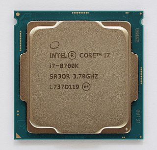
Coffee Lake is Intel's codename for its eighth-generation Core microprocessor family, announced on September 25, 2017. It is manufactured using Intel's second 14 nm process node refinement. Desktop Coffee Lake processors introduced i5 and i7 CPUs featuring six cores and Core i3 CPUs with four cores and no hyperthreading.
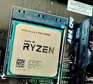
Ryzen is a brand of multi-core x86-64 microprocessors designed and marketed by Advanced Micro Devices (AMD) for desktop, mobile, server, and embedded platforms based on the Zen microarchitecture. It consists of central processing units (CPUs) marketed for mainstream, enthusiast, server, and workstation segments and accelerated processing units (APUs) marketed for mainstream and entry-level segments and embedded systems applications.
Zen 4 is the codename for a CPU microarchitecture designed by AMD, released on September 27, 2022. It is the successor to Zen 3 and uses TSMC's N6 process for I/O dies, N5 process for CCDs, and N4 process for APUs. Zen 4 powers Ryzen 7000 performance desktop processors, Ryzen 8000G series mainstream desktop APUs, and Ryzen Threadripper 7000 series HEDT and workstation processors. It is also used in extreme mobile processors, thin & light mobile processors, as well as EPYC 8004/9004 server processors.
Intel Xe, earlier known unofficially as Gen12, is a GPU architecture developed by Intel.
Sunny Cove is a codename for a CPU microarchitecture developed by Intel, first released in September 2019. It succeeds the Palm Cove microarchitecture and is fabricated using Intel's 10 nm process node. The microarchitecture is implemented in 10th-generation Intel Core processors for mobile and third generation Xeon scalable server processors. 10th-generation Intel Core mobile processors were released in September 2019, while the Xeon server processors were released on April 6, 2021.
Rocket Lake is Intel's codename for its 11th generation Core microprocessors. Released on March 30, 2021, it is based on the new Cypress Cove microarchitecture, a variant of Sunny Cove backported to Intel's 14 nm process node. Rocket Lake cores contain significantly more transistors than Skylake-derived Comet Lake cores.
Tremont is a microarchitecture for low-power Atom, Celeron and Pentium Silver branded processors used in systems on a chip (SoCs) made by Intel. It is the successor to Goldmont Plus. Intel officially launched Elkhart Lake platform with 10 nm Tremont core on September 23, 2020. Intel officially launched Jasper Lake platform with 10 nm Tremont core on January 11, 2021.
Alder Lake is Intel's codename for the 12th generation of Intel Core processors based on a hybrid architecture utilizing Golden Cove performance cores and Gracemont efficient cores. It is fabricated using Intel's Intel 7 process, previously referred to as Intel 10 nm Enhanced SuperFin (10ESF). The 10ESF has a 10%-15% boost in performance over the 10SF used in the mobile Tiger Lake processors. Intel officially announced 12th Gen Intel Core CPUs on October 27, 2021, mobile CPUs and non-K series desktop CPUs on January 4, 2022, Alder Lake-P and -U series on February 23, 2022, and Alder Lake-HX series on May 10, 2022.
Gracemont is a microarchitecture for low-power processors used in systems on a chip (SoCs) made by Intel, and is the successor to Tremont. Like its predecessor, it is also implemented as low-power cores in a hybrid design of the Alder Lake, Raptor Lake and Raptor Lake Refresh processors.
Raptor Lake is Intel's codename for the 13th and 14th generations of Intel Core processors based on a hybrid architecture, utilizing Raptor Cove performance cores and Gracemont efficient cores. Like Alder Lake, Raptor Lake is fabricated using Intel's Intel 7 process. Raptor Lake features up to 24 cores and 32 threads and is socket compatible with Alder Lake systems. Like earlier generations, Raptor Lake processors also need accompanying chipsets.
Apple M2 is a series of ARM-based system on a chip (SoC) designed by Apple Inc. as a central processing unit (CPU) and graphics processing unit (GPU) for its Mac desktops and notebooks, the iPad Pro and iPad Air tablets, and the Vision Pro mixed reality headset. It is the second generation of ARM architecture intended for Apple's Mac computers after switching from Intel Core to Apple silicon, succeeding the M1. Apple announced the M2 on June 6, 2022, at Worldwide Developers Conference (WWDC), along with models of the MacBook Air and the 13-inch MacBook Pro using the M2. The M2 is made with TSMC's "Enhanced 5-nanometer technology" N5P process and contains 20 billion transistors, a 25% increase from the M1. Apple claims CPU improvements up to 18% and GPU improvements up to 35% compared to the M1.
This new node is called Intel 4. For all practical purposes, it is the proper 10-nanometer successor. In other words, had it been released in 2020, it would have properly been called "7nm". Today, it is called 'Intel 4' and is the successor to 'Intel 7' (formerly known as '10nm Enhanced SuperFin', formerly '10nm++').