
Athlon is the brand name applied to a series of x86-compatible microprocessors designed and manufactured by AMD. The original Athlon was the first seventh-generation x86 processor and the first desktop processor to reach speeds of one gigahertz (GHz). It made its debut as AMD's high-end processor brand on June 23, 1999. Over the years AMD has used the Athlon name with the 64-bit Athlon 64 architecture, the Athlon II, and Accelerated Processing Unit (APU) chips targeting the Socket AM1 desktop SoC architecture, and Socket AM4 Zen microarchitecture. The modern Zen-based Athlon with a Radeon Graphics processor was introduced in 2019 as AMD's highest-performance entry-level processor.

Celeron is a discontinued series of low-end IA-32 and x86-64 computer microprocessor models targeted at low-cost personal computers, manufactured by Intel. The first Celeron-branded CPU was introduced on April 15, 1998, and was based on the Pentium II.

Pentium 4 is a series of single-core CPUs for desktops, laptops and entry-level servers manufactured by Intel. The processors were shipped from November 20, 2000 until August 8, 2008. It was removed from the official price lists starting in 2010, being replaced by Pentium Dual-Core.

The Pentium II brand refers to Intel's sixth-generation microarchitecture ("P6") and x86-compatible microprocessors introduced on May 7, 1997. Containing 7.5 million transistors, the Pentium II featured an improved version of the first P6-generation core of the Pentium Pro, which contained 5.5 million transistors. However, its L2 cache subsystem was a downgrade when compared to the Pentium Pros. It is a single-core microprocessor.

The Pentium III brand refers to Intel's 32-bit x86 desktop and mobile CPUs based on the sixth-generation P6 microarchitecture introduced on February 28, 1999. The brand's initial processors were very similar to the earlier Pentium II-branded processors. The most notable differences were the addition of the Streaming SIMD Extensions (SSE) instruction set, and the introduction of a controversial serial number embedded in the chip during manufacturing. The Pentium III is also a single-core processor.

The Pentium Pro is a sixth-generation x86 microprocessor developed and manufactured by Intel and introduced on November 1, 1995. It introduced the P6 microarchitecture and was originally intended to replace the original Pentium in a full range of applications. Later, it was reduced to a more narrow role as a server and high-end desktop processor. The Pentium Pro was also used in supercomputers, most notably ASCI Red, which used two Pentium Pro CPUs on each computing nodes and was the first computer to reach over one teraFLOPS in 1996, topping the number one spot in the TOP500 list from 1997 to 2000.
The Pentium M is a family of mobile 32-bit single-core x86 microprocessors introduced in March 2003 and forming a part of the Intel Carmel notebook platform under the then new Centrino brand. The Pentium M processors had a maximum thermal design power (TDP) of 5–27 W depending on the model, and were intended for use in laptops. They evolved from the core of the last Pentium III–branded CPU by adding the front-side bus (FSB) interface of Pentium 4, an improved instruction decoding and issuing front end, improved branch prediction, SSE2 support, and a much larger cache.
Tejas was a code name for Intel's microprocessor, which was to be a successor to the latest Pentium 4 with the Prescott core and was sometimes referred to as Pentium V. Jayhawk was a code name for its Xeon counterpart. The cancellation of the processors in May 2004 underscored Intel's historical transition of its focus on single-core processors to multi-core processors.

Xeon is a brand of x86 microprocessors designed, manufactured, and marketed by Intel, targeted at the non-consumer workstation, server, and embedded markets. It was introduced in June 1998. Xeon processors are based on the same architecture as regular desktop-grade CPUs, but have advanced features such as support for error correction code (ECC) memory, higher core counts, more PCI Express lanes, support for larger amounts of RAM, larger cache memory and extra provision for enterprise-grade reliability, availability and serviceability (RAS) features responsible for handling hardware exceptions through the Machine Check Architecture (MCA). They are often capable of safely continuing execution where a normal processor cannot due to these extra RAS features, depending on the type and severity of the machine-check exception (MCE). Some also support multi-socket systems with two, four, or eight sockets through use of the Ultra Path Interconnect (UPI) bus, which replaced the older QuickPath Interconnect (QPI) bus.
The NetBurst microarchitecture, called P68 inside Intel, was the successor to the P6 microarchitecture in the x86 family of central processing units (CPUs) made by Intel. The first CPU to use this architecture was the Willamette-core Pentium 4, released on November 20, 2000 and the first of the Pentium 4 CPUs; all subsequent Pentium 4 and Pentium D variants have also been based on NetBurst. In mid-2001, Intel released the Foster core, which was also based on NetBurst, thus switching the Xeon CPUs to the new architecture as well. Pentium 4-based Celeron CPUs also use the NetBurst architecture.
The Intel Core microarchitecture is a multi-core processor microarchitecture launched by Intel in mid-2006. It is a major evolution over the Yonah, the previous iteration of the P6 microarchitecture series which started in 1995 with Pentium Pro. It also replaced the NetBurst microarchitecture, which suffered from high power consumption and heat intensity due to an inefficient pipeline designed for high clock rate. In early 2004 the new version of NetBurst (Prescott) needed very high power to reach the clocks it needed for competitive performance, making it unsuitable for the shift to dual/multi-core CPUs. On May 7, 2004 Intel confirmed the cancellation of the next NetBurst, Tejas and Jayhawk. Intel had been developing Merom, the 64-bit evolution of the Pentium M, since 2001, and decided to expand it to all market segments, replacing NetBurst in desktop computers and servers. It inherited from Pentium M the choice of a short and efficient pipeline, delivering superior performance despite not reaching the high clocks of NetBurst.

Yonah is the code name of Intel's first generation 65 nm process CPU cores, based on cores of the earlier Banias / Dothan Pentium M microarchitecture. Yonah CPU cores were used within Intel's Core Solo and Core Duo mobile microprocessor products. SIMD performance on Yonah improved through the addition of SSE3 instructions and improvements to SSE and SSE2 implementations; integer performance decreased slightly due to higher latency cache. Additionally, Yonah included support for the NX bit.

Pentium is a discontinued series of x86 architecture-compatible microprocessors produced by Intel. The original Pentium was first released on March 22, 1993. The name "Pentium" is originally derived from the Greek word pente (πεντε), meaning "five", a reference to the prior numeric naming convention of Intel's 80x86 processors (8086–80486), with the Latin ending -ium since the processor would otherwise have been named 80586 using that convention.

The Pentium Dual-Core brand was used for mainstream x86-architecture microprocessors from Intel from 2006 to 2009, when it was renamed to Pentium. The processors are based on either the 32-bit Yonah or 64-bit Merom-2M, Allendale, and Wolfdale-3M core, targeted at mobile or desktop computers.

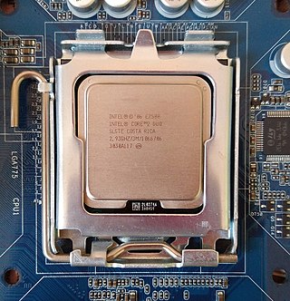
Conroe is the code name for many Intel processors sold as Core 2 Duo, Xeon, Pentium Dual-Core and Celeron. It was the first desktop processor to be based on the Core microarchitecture, replacing the NetBurst microarchitecture based Cedar Mill processor. It has product code 80557, which is shared with Allendale and Conroe-L that are very similar but have a smaller L2 cache. Conroe-L has only one processor core and a new CPUID model. The mobile version of Conroe is Merom, the dual-socket server version is Woodcrest, the quad-core desktop version is Kentsfield and the quad-core dual-socket version is Clovertown. Conroe was replaced by the 45 nm Wolfdale processor.
Wolfdale is the code name for a processor from Intel that is sold in varying configurations as Core 2 Duo, Celeron, Pentium and Xeon. In Intel's Tick-Tock cycle, the 2007/2008 "Tick" was Penryn microarchitecture, the shrink of the Merom microarchitecture to 45 nanometers as CPUID model 23. This replaced the Conroe processor with Wolfdale.
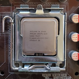
Yorkfield is the code name for some Intel processors sold as Core 2 Quad and Xeon. In Intel's Tick-Tock cycle, the 2007/2008 "Tick" was Penryn microarchitecture, the shrink of the Core microarchitecture to 45 nanometers as CPUID model 23, replacing Kentsfield, the previous model.
In Intel's Tick-Tock cycle, the 2007/2008 "Tick" was the shrink of the Core microarchitecture to 45 nanometers as CPUID model 23. In Core 2 processors, it is used with the code names Penryn, Wolfdale and Yorkfield, some of which are also sold as Celeron, Pentium and Xeon processors. In the Xeon brand, the Wolfdale-DP and Harpertown code names are used for LGA 771 based MCMs with two or four active Wolfdale cores.

