Sandy Bridge

Last updated
Sandy Bridge
Intel i5-2500.jpg
Top of a Core i5-2500
General information
LaunchedJanuary 9, 2011;13 years ago (January 9, 2011)
DiscontinuedSeptember 27, 2013 [1]
Marketed byIntel
Designed byIntel
Common manufacturer(s)
  • Intel
Product code80619 (extreme desktop)
80620 (server LGA1356)
80621 (server LGA2011)
80623 (desktop)
80627 (mobile)
Performance
Max. CPU clock rate 1.60 GHz to 3.60 GHz
QPI speeds6.4 GT/s to 8.0 GT/s
DMI speeds4 GT/s
Cache
L1 cache 64  KB per core
L2 cache256 KB per core
L3 cache1 MB to 8 MB shared
10 MB to 15 MB (Extreme)
3 MB to 20 MB (Xeon)
Architecture and classification
Microarchitecture Sandy Bridge
Instruction set x86-64
Instructions x86-16, IA-32, x86-64
Extensions
Physical specifications
Transistors
Cores
  • 1–4 (4-6 Extreme, 2-8 Xeon)
GPU(s) HD Graphics
650  MHz to 1100 MHz
HD Graphics 2000
650  MHz to 1250 MHz
HD Graphics 3000
650 MHz to 1350 MHz
HD Graphics P3000
850 MHz to 1350 MHz
Socket(s)
Products, models, variants
Product code name(s)
  • Gesher
Model(s)
  • Celeron
    Pentium
    Core i3/i5/i7/i7 Extreme
    Xeon E3/E5
History
Predecessor(s) Nehalem (Tock)
Westmere (Tick)
Successor(s) Ivy Bridge (Tick)
Haswell (Tock)
Support status
Unsupported
Bottom view of a Core i7-2600K Intel CPU Core i7 2600K Sandy Bridge perspective.jpg
Bottom view of a Core i7-2600K

Sandy Bridge is the codename for Intel's 32 nm microarchitecture used in the second generation of the Intel Core processors (Core i7, i5, i3). The Sandy Bridge microarchitecture is the successor to Nehalem and Westmere microarchitecture. Intel demonstrated an A1 stepping Sandy Bridge processor in 2009 during Intel Developer Forum (IDF), and released first products based on the architecture in January 2011 under the Core brand. [2] [3]

Contents

Sandy Bridge is manufactured in the 32 nm process and has a soldered contact with the die and IHS (Integrated Heat Spreader), while Intel's subsequent generation Ivy Bridge uses a 22 nm die shrink and a TIM (Thermal Interface Material) between the die and the IHS.

Technology

Intel demonstrated a Sandy Bridge processor with A1 stepping at 2  GHz during the Intel Developer Forum in September 2009. [4]

Upgraded features from Nehalem include:

CPU

Translation lookaside buffer sizes [16] [17]
CachePage Size
NameLevel4 KB2 MB1 GB
DTLB1st64324
ITLB1st1288 / logical corenone
STLB2nd512nonenone
All translation lookaside buffers (TLBs) are 4-way associative.[ citation needed ]

GPU

I/O

Models and steppings

All Sandy Bridge processors with one, two, or four cores report the same CPUID model 0206A7h [18] and are closely related. The stepping number cannot be seen from the CPUID but only from the PCI configuration space. The later Sandy Bridge-E processors with up to eight cores and no graphics are using CPUIDs 0206D6h and 0206D7h. [19] Ivy Bridge CPUs all have CPUID 0306A9h to date, and are built in four different configurations differing in the number of cores, L3 cache and GPU execution units:

Die codenameCPUIDSteppingCoresGPU
EUs
L3
cache
Socket(s)
Sandy Bridge-HE-40206A7hD24128 MB LGA 1155, Socket G2,
BGA-1023, BGA-1224
Sandy Bridge-H-2J124 MB LGA 1155, Socket G2,
BGA-1023
Sandy Bridge-M-2Q063 MB
Sandy Bridge-EP-80206D6hC18none20 MB LGA 2011
0206D7hC2
Sandy Bridge-EP-40206D6hM0410 MB
0206D7hM1

Performance

List of Sandy Bridge processors

1Processors featuring Intel's HD 3000 graphics are set in bold. Other processors feature HD 2000 graphics, HD graphics (Pentium and Celeron models) or no graphics core (Graphics Clock rate indicated by N/A).

Desktop platform

[21] [22] [23]

Sandy Bridge-DT and Sandy Bridge-E
Processor
branding and model
Cores
(threads)
CPU clock rate Graphics clock rate L3
Cache
TDP Release
date (Y-M-D)
Price
(USD)
Motherboard
Normal Turbo NormalTurboSocketInterfaceMemory
Core i7
Extreme
3970X 6 (12)3.5 GHz4.0 GHz15 MB150 W2012-11-12$999 LGA
2011
DMI 2.0
40× PCIe 8 GT/s [24] [29]
Up to quad
channel
DDR3-1600 [30]
3960X 3.3 GHz3.9 GHz130 W2011-11-14
Core i7 3930K 3.2 GHz3.8 GHz12 MB$583
3820 4 (8)3.6 GHz10 MB2012-02-13 [31] $294
2700K 3.5 GHz3.9 GHz850  MHz 1350 MHz8 MB95 W2011-10-24$332 LGA
1155
DMI 2.0
16× PCIe 2.0
Up to dual
channel
DDR3-1333
2600K 3.4 GHz3.8 GHz2011-01-09$317
2600 $294
2600S 2.8 GHz65 W$306
Core i5 2550K 4 (4)3.4 GHz6 MB95 W2012-01-30$225
2500K 3.3 GHz3.7 GHz850 MHz1100 MHz2011-01-09$216
2500 $205
2500S 2.7 GHz65 W$216
2500T 2.3 GHz3.3 GHz650 MHz1250 MHz45 W
2450P 3.2 GHz3.5 GHz95 W2012-01-30$195
2400 3.1 GHz3.4 GHz850 MHz1100 MHz2011-01-09$184
2405S 2.5 GHz3.3 GHz65 W2011-05-22$205
2400S 2011-01-09$195
2380P 3.1 GHz3.4 GHz95 W2012-01-30$177
2320 3.0 GHz3.3 GHz850 MHz1100 MHz2011-09-04
2310 2.9 GHz3.2 GHz2011-05-22
2300 2.8 GHz3.1 GHz2011-01-09
2390T 2 (4)2.7 GHz3.5 GHz650 MHz3 MB35 W2011-02-20$195
Core i3 2120T 2.6 GHz2011-09-04$127
2100T 2.5 GHz2011-02-20
2115C 2.0 GHz25 W2012-05$241BGA
1284
2130 3.4 GHz850 MHz1100 MHz65 W2011-09-04$138 LGA
1155
2125 3.3 GHz$134
2120 2011-02-20$138
2105 3.1 GHz2011-05-22$134
2102 Q2 2011$127
2100 2011-02-20$117
Pentium G870 2 (2)2012-06-03$86
G860 3.0 GHz2011-09-04
G860T 2.6 GHz650 MHz35 W2012-06-03$75
G850 2.9 GHz850 MHz65 W2011-05-24$86
G840 2.8 GHz$75
G645 2.9 GHz2012-09-03$64Up to dual
channel
DDR3-1066
G640 2.8 GHz2012-06-03
G632 2.7 GHzQ3 2011
G630 2011-09-04$75
G622 2.6 GHzQ2 2011
G620 2011-05-24$64
G645T 2.5 GHz650 MHz35 W2012-09-03
G640T 2.4 GHz2012-06-03
G630T 2.3 GHz2011-09-04$70
G620T 2.2 GHz2011-05-24
Celeron G555 2.7 GHz850 MHz1000 MHz2 MB65 W2012-09-02$52
G550 2.6 GHz2012-06-03
G540 2.5 GHz2011-09-04
G530 2.4 GHz$42
G550T 2.2 GHz650 MHz35 W2012-09-02
G540T 2.1 GHz2012-06-03
G530T 2.0 GHz2011-09-04$47
G470 1 (2)1.5 MB2013-06-09$37Up to dual
channel
DDR3-1333
G465 1.9 GHz2012-09-02Up to dual
channel
DDR3-1066
G460 1.8 GHz2011-12-11
G440 1 (1)1.6 GHz1 MB2011-09-04

Suffixes to denote:

NOTE: 3970X, 3960X, 3930K, and 3820 are actually of Sandy Bridge-E edition.

Server platform

All 1600/2600/4600-series models:

Sandy Bridge-EP Xeon E5-1600/2600/4600
ModelCores
(threads)
L3
Cache
CPU clock rate InterfacesSupported
memory
TDP Release
date
Price
(USD)
Base Turbo Scalability QPI
Xeon

E5

4S

4650 8 (16)20 MB2.7 GHz3.3 GHz4 sockets

(4S)

2× 8.0 GT/s

DDR3-1600

130 WMay 14, 2012$3616
4650L 2.6 GHz3.1 GHz115 W
4640 2.4 GHz2.8 GHz95 W$2725
4620 16 MB2.2 GHz2.6 GHz2× 7.2 GT/s4× DDR3-1333$1611
4617 6 (6)15 MB2.9 GHz3.4 GHz4× DDR3-1600130 W
4610 6 (12)2.4 GHz2.9 GHz4× DDR3-133395 W$1219
4607 12 MB2.2 GHzN/A2× 6.0 GT/s4× DDR3-1066$885
4603 4 (8)10 MB2.0 GHz$551
Xeon

E5

2S

2687W 8 (16)20 MB3.1 GHz3.8 GHz2 sockets

(2S)

2× 8.0 GT/s4× DDR3-1600150 WMarch 6, 2012$1885
2690 2.9 GHz3.8 GHz135 W$2057
2680 2.7 GHz3.5 GHz130 W$1723
26892.6 GHz3.6 GHz115 WOEM
2670 3.3 GHz$1552
2665 2.4 GHz3.1 GHz$1440
2660 2.2 GHz3.0 GHz95 W$1329
2658 2.1 GHz2.4 GHz$1186
2650 2.0 GHz2.8 GHz$1107
2650L 1.8 GHz2.3 GHz70 W
2648L 2.1 GHz$1186
2667 6 (12)15MB2.9 GHz3.5 GHz130 W$1552
2640 2.5 GHz3.0 GHz2× 7.2 GT/s4× DDR3-133395 W$884
2630 2.3 GHz2.8 GHz$612
2620 2.0 GHz2.5 GHz$406
2630L 60 W$662
2628L1.8 GHzN/AJuly 22, 2013OEM
2643 4 (8)10MB3.3 GHz3.5 GHz2× 8.0 GT/s4× DDR3-1600130 WMarch 6, 2012$884
2637 2 (4)5MB3.0 GHz80 W
2618L4 (8)10MB1.8 GHzN/A2× 6.4 GT/s4× DDR3-133350 WJuly 22, 2013OEM
2609 4 (4)2.4 GHz4× DDR3-106680 WMarch 6, 2012$246
2603 1.8 GHz$202
Xeon

E5

1S

1660 6 (12)15MB3.3 GHz3.9 GHz1 socket

(1S)

N/A4× DDR3-1600130 WMarch 6, 2012$1080
1650 12MB3.2 GHz3.8 GHz$583
1620 4 (8)10MB3.6 GHz$294
1607 4 (4)3.0 GHzN/A4× DDR3-1066$244
1603 2.8 GHz$198

Suffixes to denote:

Sandy Bridge-EN Xeon E5-1400/2400
SocketModelCores
(threads)
L3
Cache
CPU clock rate InterfaceSupported
memory
TDP Release
date
Price
(USD)
Base Turbo
LGA 1356

Dual

Socket

Xeon E5 2470 8 (16)20MB2.3 GHz3.1 GHzQPI

DMI 2.0

24× PCI-E 3.0

3× DDR3-160095 WMay 14, 2012$1440
2450 2.1 GHz2.9 GHz$1106
2450L 1.8 GHz2.3 GHz70 W
2448L 2.1 GHz$1151
2449L1.4 GHz1.8 GHz50 WOEM
2440 6 (12)15MB2.4 GHz2.9 GHz3× DDR3-133395 W$834
2430 2.2 GHz2.7 GHz$551
2420 1.9 GHz2.4 GHz$388
2430L 2.0 GHz2.5 GHz60 W$662
2428L 1.8 GHz2.0 GHz$628
2418L 4 (8)10MB2.0 GHz2.1 GHz50 W$387
2407 4 (4)2.2 GHzN/A3× DDR3-106680 W$250
2403 1.8 GHz$192
LGA 1356 1428L 6 (12)15MB1.8 GHz3× DDR3-133360 W$395
1410 4 (8)10MB2.8 GHz3.2 GHz80 WN/A
Pentium 1407 2 (2)5MB2.8 GHzN/A3× DDR3-1066
1403 2.6 GHz
1405 1.2 GHz1.8 GHz40 W2012-08$143
Sandy Bridge-DT Xeon E3-1200
SocketModelCores
(threads)
CPU clock rate L3

cache

Integrated
graphics
InterfaceSupported
memory
TDP Release
date
Price
(USD)
Base Turbo
LGA 1155 Xeon

E3

1290 4 (8)3.6 GHz4.0 GHz8MBN/A DMI 2.0

20× PCIe 2.0 [32]

2× DDR3-133395 WMay 29, 2011$885
1280 3.5 GHz3.9 GHzApril 3, 2011$612
1270 3.4 GHz3.8 GHz80 W$328
1240 3.3 GHz3.7 GHz$250
1230 3.2 GHz3.6 GHz$215
1220 4 (4)3.1 GHz3.4 GHz$189
1220L 2 (4)2.2 GHz3.4 GHz3MB20 W$189
1275 4 (8)3.4 GHz3.8 GHz8MBHD Graphics P300095 W$339
1245 3.3 GHz3.7 GHz$262
1235 3.2 GHz3.6 GHz$240
1225 4 (4)3.1 GHz3.4 GHz6MB$194
1265L4 (8)2.4 GHz3.3 GHz8MB45 WOEM
1260L 2.4 GHz3.3 GHzHD Graphics 2000$294

Mobile platform

Target
segment
Processor
branding and

model

Cores /
threads
CPU clock rate Graphics clock rate L3
cache
TDP Release
date
Price
(USD)
Motherboard
Base Turbo
(1C/2C/4C)
BaseTurboInterfaceSocket
ExtremeCore i7
Extreme
2960XM 4 (8)2.7 GHz3.7/3.6/3.4 GHz650 MHz1300 MHz8 MB55 W2011-09-04$1096*DMI 2.0
*Memory: Up to
dual channel
DDR3-1600 MT/s
*PCIe 2.0
Socket G2 /
BGA-1224 [33]
2920XM 2.5 GHz3.5/3.4/3.2 GHz2011-01-05
PerformanceCore i7 2860QM 2.5 GHz3.6/3.5/3.3 GHz45 W2011-09-04$568
2820QM 2.3 GHz3.4/3.3/3.1 GHz2011-01-05
2760QM 2.4 GHz3.5/3.4/3.2 GHz6 MB2011-09-04$378
2720QM 2.2 GHz3.3/3.2/3.0 GHz2011-01-05
2715QE 2.1 GHz3.0/2.9/2.7 GHz1200 MHz
2710QE
2675QM 2.2 GHz3.1/3.0/2.8 GHz1200 MHz2011-10-02*DMI 2.0
*Memory: Up to
dual channel
DDR3-1333 MHz
*PCIe 2.0
2670QM 1100 MHz
2635QM 2.0 GHz2.9/2.8/2.6 GHz1200 MHz2011-01-05
2630QM 1100 MHz
Mainstream 2640M 2 (4)2.8 GHz3.5/3.3 GHz1300 MHz4 MB35 W2011-09-04$346 Socket G2 /
BGA-1023
(in low power and embedded products) [33]
2620M 2.7 GHz3.4/3.2 GHz2011-02-20
2649M 2.3 GHz3.2/2.9 GHz500 MHz1100 MHz25 W
2629M 2.1 GHz3.0/2.7 GHz$311
2655LE 2.2 GHz2.9/2.7 GHz650 MHz1000 MHz$346
2677M 1.8 GHz2.9/2.6 GHz350 MHz1200 MHz17 W2011-06-20$317
2637M 1.7 GHz2.8/2.5 GHz$289
2657M 1.6 GHz2.7/2.4 GHz1000 MHz2011-02-20$317
2617M 1.5 GHz2.6/2.3 GHz950 MHz$289
2610UE 2.4/2.1 GHz850 MHz$317
Core i5 2557M 1.7 GHz2.7/2.4 GHz1200 MHz3 MB2011-06-20$250
2537M 1.4 GHz2.3/2.0 GHz900 MHz2011-02-20
2467M 1.6 GHz2.3/2.0 GHz1150 MHz2011-06-19
2540M 2.6 GHz3.3/3.1 GHz650 MHz1300 MHz35 W2011-06-20$266
2520M 2.5 GHz3.2/3.0 GHz$225
2515E 3.1/2.8 GHz1100 MHz$266
2510E
2450M 1300 MHz2012-01$225
2435M 2.4 GHz3.0/2.7 GHz2011-10-02OEM
2430M 1200 MHz$225
2410M 2.3 GHz2.9/2.6 GHz2011-06-20
Core i3 2370M 2.4 GHz1150 MHz2012-01
2350M 2.3 GHz2011-10-02
2348M 2013-01OEM
2330E 2.2 GHz1050 MHz2011-06-19$225
2330M 1100 MHz
2328M 2012-09
2312M 2.1 GHzQ2 2011OEM
2310E 1050 MHz2011-02-20
2310M 1100 MHz
2377M 1.5 GHz350 MHz1000 MHz17 WQ3 2012$225
2375M 2012-03
2367M 1.4 GHz2011-10-02$250
2365M 2012-09$225
2357M 1.3 GHz950 MHz2011-06-19OEM
2340UE 800 MHz$250
BudgetPentium B915C 1.5 GHz15 W2012-05$138
997 2 (2)1.6 GHz350 MHz1000 MHz2 MB17 W2012-09-30$134
987 1.5 GHzQ3 2012
977 1.4 GHz2012-01
967 1.3 GHz2011-10-02
957 1.2 GHz800 MHz2011-06-19
B980 2.4 GHz650 MHz1150 MHz35 W2012-09$125
B970 2.3 GHz2012-01
B960 2.2 GHz1100 MHz2011-10-02$134
B950 2.1 GHz2011-06-19
B940 2.0 GHz
Celeron B840 1.9 GHz1000 MHz2011-09-04$86
B830 1.8 GHz1050 MHz2012-09-30
B820 [34] 1.7 GHz2012-07-29
B815 [35] 1.6 GHz2012-01
B810E 1000 MHz2011-06-19
B810 950 MHz2011-03-13
B800 1.5 GHz1000 MHz2011-06-19$80
887 350 MHz17 W09-30-2012$86
877 1.4 GHz2012-07-29
867 1.3 GHzJanuary 2012$134
857 1.2 GHz2011-07-03
847 1.1 GHz800 MHz2011-06-19
847E
807 1 (2)1.5 GHz950 MHz1.5 MB2012-07-29$70
725C 1.3 GHz10 W2012-05$74
827E 1 (1)1.4 GHz350 MHz800 MHz17 W2011-07-03$107
797 950 MHz2012-01
787 1.3 GHz2011-07-03
B7301.8 GHz650 MHz1000 MHz35 W2012-07-29$70
B720 [36] 1.7 GHz2012-01
B710 1.6 GHz2011-06-19
807UE 1.0 GHz350 MHz800 MHz1 MB10 W2011-11$117

Suffixes to denote:

Cougar Point chipset flaw

On 31 January 2011, Intel issued a recall on all 67-series motherboards due to a flaw in the Cougar Point Chipset. [37] A hardware problem exists, in which the chipset's SATA II ports may fail over time, causing failure of connection to SATA devices, though data is not at risk. [38] Intel claims that this problem will affect only 5% of users over 3 years; however, heavier I/O workloads can exacerbate the problem. This hardware bug cannot be fixed by BIOS update.

Intel stopped production of flawed B2 stepping chipsets and began producing B3 stepping chipsets with the silicon fix. Shipping of these new chipsets started on 14 February 2011 and Intel estimated full recovery volume in April 2011. [39] Motherboard manufacturers (such as ASUS and Gigabyte Technology) and computer manufacturers (such as Dell and Hewlett-Packard) stopped selling products that involved the flawed chipset and offered support for affected customers. Options ranged from swapping for B3 motherboards to product refunds. [40] [41]

Sandy Bridge processor sales were temporarily on hold, as one cannot use the CPU without a motherboard. However, processor release dates were not affected. [42] After two weeks, Intel continued shipping some chipsets, but manufacturers had to agree to a set of terms that will prevent customers from encountering the bug. [43]

Limitations

Overclocking

With Sandy Bridge, Intel has tied the speed of every bus (USB, SATA, PCI, PCIe, CPU cores, Uncore, memory etc.) to a single internal clock generator issuing the basic 100 MHz Base Clock (BClk). [44] With CPUs being multiplier locked, the only way to overclock is to increase the BClk, which can be raised by only 5–7% without other hardware components failing. As a work around, Intel made available K/X-series processors, which feature unlocked multipliers; with a multiplier cap of 57 for Sandy Bridge. [45] For the Sandy Bridge-E platform, there is alternative method known as the BClk ratio overclock. [46]

During IDF (Intel Developer Forum) 2010, Intel demonstrated an unknown Sandy Bridge CPU running stably overclocked at 4.9 GHz on air cooling. [47] [48]

Chipset

Non-K edition CPUs can overclock up to four bins from its turbo multiplier. Refer here for chipset support.

vPro remote-control

Sandy and Ivy Bridge processors with vPro capability have security features that can remotely disable a PC or erase information from hard drives. This can be useful in the case of a lost or stolen PC. The commands can be received through 3G signals, Ethernet, or Internet connections. AES encryption acceleration will be available, which can be useful for video conferencing and VoIP applications. [49] [50]

Intel Insider

Sandy and Ivy Bridge processors contain a DRM technology that some video streaming web sites rely on to restrict use of their content. Such web sites offer 1080p streaming to users with such CPUs and downgrade the quality for other users. [51]

Software development kit

With the introduction of the Sandy Bridge microarchitecture, Intel also introduced the Intel Data Plane Development Kit (Intel DPDK) to help developers of communications applications take advantage of the platform in packet processing applications, and network processors. [52]

Roadmap

Intel demonstrated the Haswell architecture in September 2011, released in 2013 as the successor to Sandy Bridge and Ivy Bridge. [53]

Fixes

In 2015, Microsoft released a microcode update for selected Sandy Bridge and Ivy Bridge CPUs for Windows 7 and up that addresses stability issues. However, the update negatively impacts Pentium G3258 and Core i3-4010U CPU models. [54] [55] [56]

See also

Related Research Articles

<span class="mw-page-title-main">Xeon</span> Line of Intel server and workstation processors

Xeon is a brand of x86 microprocessors designed, manufactured, and marketed by Intel, targeted at the non-consumer workstation, server, and embedded markets. It was introduced in June 1998. Xeon processors are based on the same architecture as regular desktop-grade CPUs, but have advanced features such as support for error correction code (ECC) memory, higher core counts, more PCI Express lanes, support for larger amounts of RAM, larger cache memory and extra provision for enterprise-grade reliability, availability and serviceability (RAS) features responsible for handling hardware exceptions through the Machine Check Architecture (MCA). They are often capable of safely continuing execution where a normal processor cannot due to these extra RAS features, depending on the type and severity of the machine-check exception (MCE). Some also support multi-socket systems with two, four, or eight sockets through use of the Ultra Path Interconnect (UPI) bus, which replaced the older QuickPath Interconnect (QPI) bus.

<span class="mw-page-title-main">Northbridge (computing)</span> PC chip handling onboard control tasks

In computing, a northbridge is a microchip that comprises the core logic chipset architecture on motherboards to handle high-performance tasks, especially for older personal computers. It is connected directly to a CPU via the front-side bus (FSB), and is usually used in conjunction with a slower southbridge to manage communication between the CPU and other parts of the motherboard.

<span class="mw-page-title-main">Nehalem (microarchitecture)</span> CPU microarchitecture by Intel

Nehalem is the codename for Intel's 45 nm microarchitecture released in November 2008. It was used in the first generation of the Intel Core i5 and i7 processors, and succeeds the older Core microarchitecture used on Core 2 processors. The term "Nehalem" comes from the Nehalem River.

<span class="mw-page-title-main">LGA 1366</span> CPU socket for Intel processors

LGA 1366, also known as Socket B, is an Intel CPU socket. This socket supersedes Intel's LGA 775 in the high-end and performance desktop segments. It also replaces the server-oriented LGA 771 in the entry level and is superseded itself by LGA 2011. This socket has 1,366 protruding pins which touch contact points on the underside of the processor (CPU) and accesses up to three channels of DDR3 memory via the processor's internal memory controller.

<span class="mw-page-title-main">Haswell (microarchitecture)</span> Intel processor microarchitecture

Haswell is the codename for a processor microarchitecture developed by Intel as the "fourth-generation core" successor to the Ivy Bridge. Intel officially announced CPUs based on this microarchitecture on June 4, 2013, at Computex Taipei 2013, while a working Haswell chip was demonstrated at the 2011 Intel Developer Forum. Haswell was the last generation of Intel processor to have socketed processors on mobile. With Haswell, which uses a 22 nm process, Intel also introduced low-power processors designed for convertible or "hybrid" ultrabooks, designated by the "U" suffix. Haswell began shipping to manufacturers and OEMs in mid-2013, with its desktop chips officially launched in September 2013.

Lynnfield is the code name for a quad-core processor from Intel released in September 2009. It was sold in varying configurations as Core i5-7xx, Core i7-8xx or Xeon X34xx. Lynnfield uses the Nehalem microarchitecture and replaces the earlier Penryn based Wolfdale and Yorkfield processors, using the same 45 nm process technology, but with a new memory and bus interface. The product code for Lynnfield is 80605, its CPUID value identifies it as family 6, model 30 (0106Ex).

<span class="mw-page-title-main">Arrandale</span> Family of computer processors by Intel

Arrandale is the code name for a family of mobile Intel processors, sold as mobile Intel Core i3, i5 and i7 as well as Celeron and Pentium. It is closely related to the desktop Clarkdale processor; both use dual-core dies based on the Westmere 32 nm die shrink of the Nehalem microarchitecture, and have integrated Graphics as well as PCI Express and DMI links.

<span class="mw-page-title-main">Intel Core</span> Line of CPUs by Intel

Intel Core is a line of multi-core central processing units (CPUs) for midrange, embedded, workstation, high-end and enthusiast computer markets marketed by Intel Corporation. These processors displaced the existing mid- to high-end Pentium processors at the time of their introduction, moving the Pentium to the entry level. Identical or more capable versions of Core processors are also sold as Xeon processors for the server and workstation markets.

<span class="mw-page-title-main">Intel Graphics Technology</span> Series of integrated graphics processors by Intel

Intel Graphics Technology (GT) is the collective name for a series of integrated graphics processors (IGPs) produced by Intel that are manufactured on the same package or die as the central processing unit (CPU). It was first introduced in 2010 as Intel HD Graphics and renamed in 2017 as Intel UHD Graphics.

<span class="mw-page-title-main">LGA 2011</span> CPU socket created by Intel

LGA 2011, also called Socket R, is a CPU socket by Intel released on November 14, 2011. It launched along with LGA 1356 to replace its predecessor, LGA 1366 and LGA 1567. While LGA 1356 was designed for dual-processor or low-end servers, LGA 2011 was designed for high-end desktops and high-performance servers. The socket has 2011 protruding pins that touch contact points on the underside of the processor.

<span class="mw-page-title-main">Skylake (microarchitecture)</span> CPU microarchitecture by Intel

Skylake is Intel's codename for its sixth generation Core microprocessor family that was launched on August 5, 2015, succeeding the Broadwell microarchitecture. Skylake is a microarchitecture redesign using the same 14 nm manufacturing process technology as its predecessor, serving as a tock in Intel's tick–tock manufacturing and design model. According to Intel, the redesign brings greater CPU and GPU performance and reduced power consumption. Skylake CPUs share their microarchitecture with Kaby Lake, Coffee Lake, Whiskey Lake, and Comet Lake CPUs.

Intel Quick Sync Video is Intel's brand for its dedicated video encoding and decoding hardware core. Quick Sync was introduced with the Sandy Bridge CPU microarchitecture on 9 January 2011 and has been found on the die of Intel CPUs ever since.

<span class="mw-page-title-main">Ivy Bridge (microarchitecture)</span> CPU microarchitecture by Intel

Ivy Bridge is the codename for Intel's 22 nm microarchitecture used in the third generation of the Intel Core processors. Ivy Bridge is a die shrink to 22 nm process based on FinFET ("3D") Tri-Gate transistors, from the former generation's 32 nm Sandy Bridge microarchitecture—also known as tick–tock model. The name is also applied more broadly to the Xeon and Core i7 Extreme Ivy Bridge-E series of processors released in 2013.

<span class="mw-page-title-main">Broadwell (microarchitecture)</span> Fifth generation of Intel Core processors

Broadwell is the fifth generation of the Intel Core processor. It is Intel's codename for the 14 nanometer die shrink of its Haswell microarchitecture. It is a "tick" in Intel's tick–tock principle as the next step in semiconductor fabrication. Like some of the previous tick-tock iterations, Broadwell did not completely replace the full range of CPUs from the previous microarchitecture (Haswell), as there were no low-end desktop CPUs based on Broadwell.

<span class="mw-page-title-main">LGA 1151</span> Intel microprocessor compatible socket

LGA 1151, also known as Socket H4, is a type of zero insertion force flip-chip land grid array (LGA) socket for Intel desktop processors which comes in two distinct versions: the first revision which supports both Intel's Skylake and Kaby Lake CPUs, and the second revision which supports Coffee Lake CPUs exclusively.

<span class="mw-page-title-main">Kaby Lake</span> Intel microprocessor, released in 2016

Kaby Lake is Intel's codename for its seventh generation Core microprocessor family announced on August 30, 2016. Like the preceding Skylake, Kaby Lake is produced using a 14 nanometer manufacturing process technology. Breaking with Intel's previous "tick–tock" manufacturing and design model, Kaby Lake represents the optimized step of the newer process–architecture–optimization model. Kaby Lake began shipping to manufacturers and OEMs in the second quarter of 2016, with its desktop chips officially launched in January 2017.

<span class="mw-page-title-main">Coffee Lake</span> Eighth-generation Intel Core microprocessor family

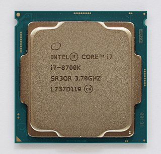
Coffee Lake is Intel's codename for its eighth-generation Core microprocessor family, announced on September 25, 2017. It is manufactured using Intel's second 14 nm process node refinement. Desktop Coffee Lake processors introduced i5 and i7 CPUs featuring six cores and Core i3 CPUs with four cores and no hyperthreading.

Rocket Lake is Intel's codename for its 11th generation Core microprocessors. Released on March 30, 2021, it is based on the new Cypress Cove microarchitecture, a variant of Sunny Cove backported to Intel's 14 nm process node. Rocket Lake cores contain significantly more transistors than Skylake-derived Comet Lake cores.

Raptor Lake is Intel's codename for the 13th and 14th generations of Intel Core processors based on a hybrid architecture, utilizing Raptor Cove performance cores and Gracemont efficient cores. Like Alder Lake, Raptor Lake is fabricated using Intel's Intel 7 process. Raptor Lake features up to 24 cores and 32 threads and is socket compatible with Alder Lake systems. Like earlier generations, Raptor Lake processors also need accompanying chipsets.

References

  1. Shvets, Gennadiy (September 26, 2012). "Intel discontinues second-generation Core i5 and i7 CPUs". CPU World. Retrieved 2020-07-29.
  2. "The Man Behind 'Sandy Bridge'". December 28, 2010. Archived from the original on December 2, 2011. Retrieved November 11, 2011.
  3. Brooke Crothers (December 15, 2010). "CES: First Intel next-gen laptops will be quad core". The Circuits Blog. CNET.com. Archived from the original on February 20, 2014. Retrieved November 11, 2011.
  4. Anand Lal Shimpi (September 22, 2009). "IDF 2009 – Intel Shows off 22nm & 32nm, Sandy Bridge Demoed". AnandTech . Retrieved November 11, 2011.
  5. "Archived copy" (PDF). Archived from the original (PDF) on 2019-01-01. Retrieved 2015-11-30.{{cite web}}: CS1 maint: archived copy as title (link)
  6. Chris Angelini (3 January 2011). "The System Agent And Turbo Boost 2.0". Tom's Hardware.
  7. "Intel Turbo Boost Technology 2.0". Intel.
  8. Lal Shimpi, Anand (October 12, 2011). "The Bulldozer Review: AMD FX-8150 Tested". Anandtech.
  9. "Intel's Sandy Bridge Microarchitecture". RealWorldTech.com.
  10. "Intel's Sandy Bridge Microarchitecture". RealWorldTech.com.
  11. "Intel's Sandy Bridge Microarchitecture". RealWorldTech.com.
  12. "Intel's Sandy Bridge Microarchitecture". RealWorldTech.com.
  13. "Intel's Sandy Bridge Microarchitecture". RealWorldTech.com.
  14. Lal Shimpi, Anand (2012-10-05). "Intel's Haswell Architecture Analyzed". AnandTech . Retrieved 2013-10-20.
  15. "Sandy Bridge (client) - Microarchitectures - Intel - WikiChip". en.wikichip.org. Retrieved 2021-02-09.
  16. "Intel 64 and IA-32 Architectures Optimization Reference Manual". Intel.com. Intel. Retrieved 2014-01-21.
  17. "Intel 64 and IA-32 Architectures Optimization Reference Manual" (PDF). Intel.com. Intel. Retrieved 2014-01-21.
  18. "Support for the Intel Core i5 Desktop Processor". Intel.com. Intel. 2012-02-22. Retrieved 2014-01-21.
  19. "Archived copy" (PDF). Archived from the original (PDF) on 2012-03-04. Retrieved 2011-12-21.{{cite web}}: CS1 maint: archived copy as title (link)
  20. Anand Lal Shimpi. "The Sandy Bridge Review: Intel Core i7-2600K, i5-2500K and Core i3-2100 Tested". anandtech.com. Retrieved 27 May 2015.
  21. "Intel's Sandy Bridge E-Series in Q4 2011". Tom's Hardware. 2011-02-11. Retrieved 2011-02-13.
  22. "Additional Details on Sandy Bridge-E Processors, X79, and LGA2011". Anandtech. 2011-04-26. Retrieved 2011-04-30.
  23. "Products (Formerly Sandy Bridge)". Official product web site. Intel. Retrieved November 11, 2011.
  24. "Intel® Core™ i7 Processor Family for the LGA-2011 Socket Datasheet, Volume 1" (PDF). Intel. p. 8: "The processor features up to 40 lanes of PCI Express links capable of up to 8.0 GT/s, and 4 lanes of DMI2/PCI Express 2.0 interface with a peak transfer rate of 5.0 GT/s. "
    p. 10: "Support for PCI Express 2.0 (5.0 GT/s), PCI Express (2.5 GT/s), and capable of up to PCI Express 8.0 GT/s. Up to 40 lanes of PCI Express interconnect for general purpose PCI Express devices capable of up to 8.0 GT/s speeds that are configurable for up to 10 independent ports."
  25. Nita, Sorin (October 17, 2011). "Intel Sandy Bridge-E CPUs Are 'Almost' PCI Express 3.0 Compatible". Softpedia .
  26. Angelini, Chris (November 14, 2011). "Intel Core i7-3960X Review: Sandy Bridge-E And X79 Express". Tom's Hardware . p. 2. It turns out that PCI Express 3.0 is, in fact, supported by Sandy Bridge-E (and the preview was updated to confirm 8 GT/s support the day after it went live). But because there weren't (and still aren't) any third-gen devices available yet, validating the feature was problematic. In fact, as you can see in the image below, Intel is still only officially guaranteeing that PCI Express 2.0 works, and probably will continue to do so until we see some hardware with a third-gen interface. Nevertheless, Intel's Core i7 datasheet confirms PCI Express 3.0 compliance, enabling up to 1 GB/s of bandwidth per lane, per direction.
  27. Shimpi, Anand Lal (December 22, 2011). "Sandy Bridge E & X79 PCIe 3.0: It Works". AnandTech .
  28. "Sandy Bridge-E and PCI-E 3.0". Intel Community Product Support.
  29. Shortly before Sandy Bridge-E's release, [25] Intel decided not to claim its PCIe 3.0 support, because the lack of any PCIe 3.0-certified hardware at the time of release would make it difficult to validate compliance. However the ability to operate in the 3.0 mode was preserved, which was confirmed by media and acknowledged by Intel. [26] [27] [28]
  30. Angelini, Chris (September 12, 2011). "Intel Core i7-3960X (Sandy Bridge-E) And X79 Platform Preview". Tom's Hardware. Retrieved November 14, 2011.
  31. Fuad Abazovic (January 6, 2012). "Intel Core i7-3820 comes on February 13". Fudzilla. Archived from the original on January 8, 2012. Retrieved January 6, 2012.
  32. Angelini, Chris (May 3, 2011). "Intel Xeon E3-1275 Review: Sandy Bridge Goes Professional". Tom's Hardware . p. 3.
  33. 1 2 "2nd Generation Intel Core i7 Processors". Ark.intel.com. Retrieved 2014-01-21.
  34. "Intel Mobile Celeron B820 - FF8062700848602". Cpu-world.com. Retrieved 2014-01-21.
  35. "Intel Mobile Celeron B815 - FF8062701159901". Cpu-world.com. Retrieved 2014-01-21.
  36. "Intel Mobile Celeron B720 - FF8062701084101". Cpu-world.com. Retrieved 2014-01-21.
  37. محمد رضا پناهی (8 February 2011). "Sandy Bridge، راه حل‌ها، بازار ایران". سخت افزار: مشاوره و بررسی گجت های دیجیتال. Retrieved 27 May 2015.
  38. "Intel Identifies Cougar Point Chipset Error, Halts Shipments". Tom's Hardware. 31 January 2011.
  39. "Intel Identifies Chipset Design Error, Implementing Solution" (Press release). Intel Corporation. January 31, 2011.
  40. "Intel chip bug affects HP, Dell, Samsung and Lenovo". BBC News. 2011-02-03.
  41. "HP to offer refund for PCs with flawed Intel chip". Reuters. 2011-02-02.
  42. "Intel to Ship Dual-core Sandy Bridge Chips on Feb. 20". PCWorld. 7 February 2011. Retrieved 27 May 2015.
  43. "Intel to continue shipping flawed Sandy Bridge chipsets". Expert Reviews. Retrieved 27 May 2015.
  44. Intel to limit Sandy Bridge Overclocking, Bit-Tech, July 22, 2010
  45. Anand Lal Shimpi (September 14, 2010). "Intel's Sandy Bridge Architecture Exposed". AnandTech . p. 8. Retrieved November 11, 2011.
  46. "Intel Core i7-3820 Extreme Edition CPU | Intel, Core i7-3820, CPU, Extreme Edition, Desktop, Processor, BX80619i73820, Benchmarks, Performance, Tests, Hank Tolman, Intel Core i7-3820 CPU Extreme Edition Desktop Processor BX80619i73820 Benchmark Performance Tests by Hank Tolman". Benchmarkreviews.com. 2012-03-05. Retrieved 2014-01-21.
  47. YouTube. youtube.com. Archived from the original on 2011-01-04. Retrieved 27 May 2015.
  48. "IDF Intel 2010: Intel Overclocks Sandy Bridge CPU to 4.9 GHz, outpaces 12-core AMD Opteron". ZDNet. Archived from the original on 2010-09-21.
  49. Hachman, Mark (2010-09-14). "Intel's 'Sandy Bridge' Chip to Include vPro Business Features". PC Magazine.
  50. "Intel vPro Technology". Intel.
  51. "Intel Insider". Intel.
  52. Rick Merritt, Intel targets data plane with comms Soc, EE Times, February 2012
  53. Crothers, Brooke (September 14, 2011). "Haswell chip completes Ultrabook 'revolution'". The Circuits Blog. CNET.com. Retrieved November 11, 2011.
  54. "June 2015 Intel CPU microcode update for Windows" . Retrieved 2020-11-07.
  55. "Windows 7: June 2015 microcode update for Intel processors in Windows" . Retrieved 2020-11-07.
  56. "Windows update KB3064209 (G3258 & 4010U)" . Retrieved 2020-11-07.

Further reading