NetBurst

Last updated

NetBurst
General information
LaunchedNovember 20, 2000;23 years ago (November 20, 2000)
Performance
Max. CPU clock rate 1.3 GHz to 3.8 GHz
FSB speeds100 MT/s to 1066 MT/s
Cache
L1 cache 8 KB to 16 KB per core
L2 cache128 KB to 4096 KB
L3 cache4 MB to 16 MB shared
Architecture and classification
Microarchitecture NetBurst
Instruction set x86-16, IA-32,
x86-64 (some)
Extensions
Physical specifications
Transistors
Cores
  • 1-2 (2-4 threads with hyper-threading)
Socket(s)
Products, models, variants
Model(s)
  • Celeron
  • Celeron D
  • Pentium 4
  • Pentium D
  • Xeon
History
Predecessor(s) P6
Successor(s) Intel Core
IA-64

The NetBurst microarchitecture, [1] [2] called P68 inside Intel, was the successor to the P6 microarchitecture in the x86 family of central processing units (CPUs) made by Intel. The first CPU to use this architecture was the Willamette-core Pentium 4, released on November 20, 2000 and the first of the Pentium 4 CPUs; all subsequent Pentium 4 and Pentium D variants have also been based on NetBurst. In mid-2001, Intel released the Foster core, which was also based on NetBurst, thus switching the Xeon CPUs to the new architecture as well. Pentium 4-based Celeron CPUs also use the NetBurst architecture.

Contents

NetBurst was replaced with the Core microarchitecture based on P6, released in July 2006.

Technology

The NetBurst microarchitecture includes features such as Hyper-threading, Hyper Pipelined Technology, Rapid Execution Engine, Execution Trace Cache, and replay system which all were introduced for the first time in this particular microarchitecture, and some never appeared again afterwards.

Hyper-threading

Hyper-threading is Intel's proprietary simultaneous multithreading (SMT) implementation used to improve parallelization of computations (doing multiple tasks at once) performed on x86 processors. Intel introduced it with NetBurst processors in 2002. Later Intel reintroduced it in the Nehalem microarchitecture after its absence in the Core 2.

Quad-Pumped Front-Side Bus

The Northwood and Willamette cores feature an external Front Side Bus (FSB) that runs at 100 MHz which transfers four bits per clock cycle, thus having an effective speed of 400 MHz. Later revisions of the Northwood core, along with the Prescott core (and derivatives) have an effective 800 MHz front-side bus (200 MHz quad pumped).

Hyper-Pipelined Technology

The Wilamette and Northwood cores contain a 20-stage instruction pipeline. This is a significant increase in the number of stages compared to the Pentium III, which had only 10 stages in its pipeline. The Prescott core increased the length of the pipeline to 31 stages. A drawback of longer pipelines is the increase in the number of stages that need to be traced back in the event that the branch misprediction, increasing the penalty of said misprediction. To address this issue, Intel devised the Rapid Execution Engine and has invested a great deal into its branch prediction technology, which Intel claims reduces branch mispredictions by 33% over Pentium III. [3] In reality, the longer pipeline resulted in reduced efficiency through a lower number of instructions per clock (IPC) executed as high enough clock speeds were not able to be reached to offset lost performance due to larger than expected increase in power consumption and heat.

Rapid Execution Engine

With this technology, the two arithmetic logic units (ALUs) in the core of the CPU are double-pumped, meaning that they actually operate at twice the core clock frequency. For example, in a 3.8 GHz processor, the ALUs will effectively be operating at 7.6 GHz. The reason behind this is to generally make up for the low IPC count; additionally this considerably enhances the integer performance of the CPU. Intel also replaced the high-speed barrel shifter with a shift/rotate execution unit that operates at the same frequency as the CPU core. The downside is that certain instructions are now much slower (relatively and absolutely) than before, making optimization for multiple target CPUs difficult. An example is shift and rotate operations, which suffer from the lack of a barrel shifter which was present on every x86 CPU beginning with the i386, including the main competitor processor, Athlon.

Execution Trace Cache

Within the L1 cache of the CPU, Intel incorporated its Execution Trace Cache. It stores decoded micro-operations, so that when executing a new instruction, instead of fetching and decoding the instruction again, the CPU directly accesses the decoded micro-ops from the trace cache, thereby saving considerable time. Moreover, the micro-ops are cached in their predicted path of execution, which means that when instructions are fetched by the CPU from the cache, they are already present in the correct order of execution. [4] Intel later introduced a similar but simpler concept with Sandy Bridge called micro-operation cache (UOP cache).

Replay system

The replay system is a subsystem within the Intel Pentium 4 processor to catch operations that have been mistakenly sent for execution by the processor's scheduler. Operations caught by the replay system are then re-executed in a loop until the conditions necessary for their proper execution have been fulfilled.

Branch prediction hints

The Intel NetBurst architecture allows branch prediction hints to be inserted into the code to tell whether the static prediction should be taken or not taken, while this feature was abandoned in later Intel processors. According to Intel, NetBurst's branch prediction algorithm is 33% better than the one in P6. [5] [6]

Scaling-up issues

Despite these enhancements, the NetBurst architecture created obstacles for engineers trying to scale up its performance. With this microarchitecture, Intel planned to attain clock speeds of 10 GHz, [7] but because of rising clock speeds, Intel faced increasing problems with keeping power dissipation within acceptable limits. Intel reached a speed barrier of 3.8 GHz in November 2004 but encountered problems trying to achieve even that. Intel abandoned NetBurst in 2006 after the heat problems became unacceptable and then developed the Core microarchitecture, inspired by the P6 Core of the Pentium Pro to the Tualatin Pentium III-S, and most directly the Pentium M.

Revisions

RevisionProcessor Brand(s)Pipeline stages
Willamette (180 nm)Celeron, Pentium 4, Xeon20
Northwood (130 nm)Celeron, Pentium 4, Pentium 4 HT, Pentium 4 HT Extreme Edition, Xeon20
Prescott (90 nm)Celeron D, Pentium 4, Pentium 4 HT,
Pentium 4 HT Extreme Edition, Xeon
31
Cedar Mill (65 nm)Celeron D, Pentium 4 HT31
Smithfield (90 nm)Pentium D, Xeon31
Presler (65 nm)Pentium D, Xeon31

Intel replaced the original Willamette core with a redesigned version of the NetBurst microarchitecture called Northwood in January 2002. The Northwood design combined an increased cache size, a smaller 130 nm fabrication process, and Hyper-threading (although initially all models but the 3.06 GHz model had this feature disabled) to produce a more modern, higher-performing version of the NetBurst microarchitecture.

In February 2004, Intel introduced Prescott, a more radical revision of the microarchitecture. The Prescott core was produced on a 90 nm process, and included several major design changes, including the addition of an even larger cache (from 512 KB in the Northwood to 1 MB, and 2 MB in Prescott 2M), a much deeper instruction pipeline (31 stages as compared to 20 in the Northwood), a heavily improved branch predictor, the introduction of the SSE3 instructions, and later, the implementation of Intel Extended Memory 64 Technology (EM64T), Intel's branding for their compatible implementation of the x86-64 64-bit version of the x86 microarchitecture (as with hyper-threading, all Prescott chips branded Pentium 4 HT have hardware to support this feature, but it was initially only enabled on the high-end Xeon processors, before being officially introduced in processors with the Pentium trademark). Power consumption and heat dissipation also became major issues with Prescott, which quickly became the hottest-running, and most power-hungry, of Intel's single-core x86 and x86-64 processors. Power and heat concerns prevented Intel from releasing a Prescott clocked above 3.8 GHz, along with a mobile version of the core clocked above 3.46 GHz.

Intel also released a dual-core processor based on the NetBurst microarchitecture branded Pentium D. The first Pentium D core was codenamed Smithfield, which is actually two Prescott cores in a single die, and later Presler, which consists of two Cedar Mill cores on two separate dies (Cedar Mill being the 65 nm die-shrink of Prescott).

Roadmap

Successor

Intel had Netburst-based successors in development called Tejas and Jayhawk with between 40 and 50 pipeline stages, but ultimately decided to replace NetBurst with the Core microarchitecture, [8] [9] released in July 2006; these successors were more directly derived from the Pentium Pro (P6 microarchitecture). August 8, 2008 marked the end of Intel NetBurst-based processors. [10] The reason for NetBurst's abandonment was the severe heat problems caused by high clock speeds. While some Core- and Nehalem-based processors have higher TDPs, most processors are multi-core, so each core gives off a fraction of the maximum TDP, and the highest-clocked Core-based single-core processors give off a maximum of 27 W of heat. The fastest-clocked desktop Pentium 4 processors (single-core) had TDPs of 115 W, compared to 88 W for the fastest clocked mobile versions. Although, with the introduction of new steppings, TDPs for some models were eventually lowered.

The Nehalem microarchitecture, the successor to the Core microarchitecture, was supposed to be an evolution of NetBurst according to Intel roadmaps dating back to 2000.[ citation needed ] Nehalem reimplements certain features of NetBurst, including the Hyper-Threading technology first introduced in the 3.06 GHz Northwood core, and L3 cache, first implemented on a consumer processor in the Gallatin core used in the Pentium 4 Extreme Edition.

NetBurst-based chips

See also

Related Research Articles

<span class="mw-page-title-main">Celeron</span> Line of discontinued microprocessors made by Intel

Celeron is a discontinued series of low-end IA-32 and x86-64 computer microprocessor models targeted at low-cost personal computers, manufactured by Intel. The first Celeron-branded CPU was introduced on April 15, 1998, and was based on the Pentium II.

<span class="mw-page-title-main">Hyper-threading</span> Proprietary simultaneous multithreading implementation by Intel

Hyper-threading is Intel's proprietary simultaneous multithreading (SMT) implementation used to improve parallelization of computations performed on x86 microprocessors. It was introduced on Xeon server processors in February 2002 and on Pentium 4 desktop processors in November 2002. Since then, Intel has included this technology in Itanium, Atom, and Core 'i' Series CPUs, among others.

<span class="mw-page-title-main">Pentium 4</span> Brand by Intel

Pentium 4 is a series of single-core CPUs for desktops, laptops and entry-level servers manufactured by Intel. The processors were shipped from November 20, 2000 until August 8, 2008. It was removed from the official price lists starting in 2010, being replaced by Pentium Dual-Core.

<span class="mw-page-title-main">Pentium III</span> Line of desktop and mobile microprocessors produced by Intel

The Pentium III brand refers to Intel's 32-bit x86 desktop and mobile CPUs based on the sixth-generation P6 microarchitecture introduced on February 28, 1999. The brand's initial processors were very similar to the earlier Pentium II-branded processors. The most notable differences were the addition of the Streaming SIMD Extensions (SSE) instruction set, and the introduction of a controversial serial number embedded in the chip during manufacturing. The Pentium III is also a single-core processor.

<span class="mw-page-title-main">Pentium M</span> Family of Intel microprocessors

The Pentium M is a family of mobile 32-bit single-core x86 microprocessors introduced in March 2003 and forming a part of the Intel Carmel notebook platform under the then new Centrino brand. The Pentium M processors had a maximum thermal design power (TDP) of 5–27 W depending on the model, and were intended for use in laptops. They evolved from the core of the last Pentium III–branded CPU by adding the front-side bus (FSB) interface of Pentium 4, an improved instruction decoding and issuing front end, improved branch prediction, SSE2 support, and a much larger cache.

Tejas was a code name for Intel's microprocessor, which was to be a successor to the latest Pentium 4 with the Prescott core and was sometimes referred to as Pentium V. Jayhawk was a code name for its Xeon counterpart. The cancellation of the processors in May 2004 underscored Intel's historical transition of its focus on single-core processors to multi-core processors.

<span class="mw-page-title-main">Xeon</span> Line of Intel server and workstation processors

Xeon is a brand of x86 microprocessors designed, manufactured, and marketed by Intel, targeted at the non-consumer workstation, server, and embedded markets. It was introduced in June 1998. Xeon processors are based on the same architecture as regular desktop-grade CPUs, but have advanced features such as support for error correction code (ECC) memory, higher core counts, more PCI Express lanes, support for larger amounts of RAM, larger cache memory and extra provision for enterprise-grade reliability, availability and serviceability (RAS) features responsible for handling hardware exceptions through the Machine Check Architecture (MCA). They are often capable of safely continuing execution where a normal processor cannot due to these extra RAS features, depending on the type and severity of the machine-check exception (MCE). Some also support multi-socket systems with two, four, or eight sockets through use of the Ultra Path Interconnect (UPI) bus, which replaced the older QuickPath Interconnect (QPI) bus.

<span class="mw-page-title-main">Pentium D</span> Family of Intel microprocessors

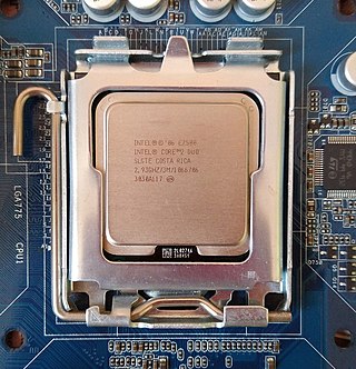
Pentium D is a range of desktop 64-bit x86-64 processors based on the NetBurst microarchitecture, which is the dual-core variant of the Pentium 4 manufactured by Intel. Each CPU comprised two cores. The brand's first processor, codenamed Smithfield and manufactured on the 90 nm process, was released on May 25, 2005, followed by the 65 nm Presler nine months later. The core implementation on the 90 nm "Smithfield" and later 65 nm "Presler" are designed differently but are functionally the same. The 90 nm "Smithfield" contains a single die, with two adjoined but functionally separate CPU cores cut from the same wafer. The later 65 nm "Presler" utilized a multi-chip module package, where two discrete dies each containing a single core reside on the CPU substrate. Neither the 90nm "Smithfield" nor the 65 nm "Presler" were capable of direct core to core communication, relying instead on the northbridge link to send information between the 2 cores.

<span class="mw-page-title-main">P6 (microarchitecture)</span> Intel processor microarchitecture

The P6 microarchitecture is the sixth-generation Intel x86 microarchitecture, implemented by the Pentium Pro microprocessor that was introduced in November 1995. It is frequently referred to as i686. It was planned to be succeeded by the NetBurst microarchitecture used by the Pentium 4 in 2000, but was revived for the Pentium M line of microprocessors. The successor to the Pentium M variant of the P6 microarchitecture is the Core microarchitecture which in turn is also derived from P6.

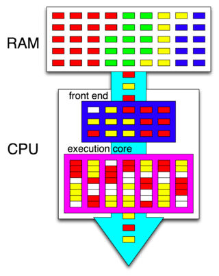
The Intel Core microarchitecture is a multi-core processor microarchitecture launched by Intel in mid-2006. It is a major evolution over the Yonah, the previous iteration of the P6 microarchitecture series which started in 1995 with Pentium Pro. It also replaced the NetBurst microarchitecture, which suffered from high power consumption and heat intensity due to an inefficient pipeline designed for high clock rate. In early 2004 the new version of NetBurst (Prescott) needed very high power to reach the clocks it needed for competitive performance, making it unsuitable for the shift to dual/multi-core CPUs. On May 7, 2004 Intel confirmed the cancellation of the next NetBurst, Tejas and Jayhawk. Intel had been developing Merom, the 64-bit evolution of the Pentium M, since 2001, and decided to expand it to all market segments, replacing NetBurst in desktop computers and servers. It inherited from Pentium M the choice of a short and efficient pipeline, delivering superior performance despite not reaching the high clocks of NetBurst.

<span class="mw-page-title-main">Yonah (microprocessor)</span> Code name of Intels first generation 65 nm process CPU cores

Yonah is the code name of Intel's first generation 65 nm process CPU cores, based on cores of the earlier Banias / Dothan Pentium M microarchitecture. Yonah CPU cores were used within Intel's Core Solo and Core Duo mobile microprocessor products. SIMD performance on Yonah improved through the addition of SSE3 instructions and improvements to SSE and SSE2 implementations; integer performance decreased slightly due to higher latency cache. Additionally, Yonah included support for the NX bit.

<span class="mw-page-title-main">Pentium</span> Brand of discontinued microprocessors produced by Intel

Pentium is a discontinued series of x86 architecture-compatible microprocessors produced by Intel. The original Pentium was first released on March 22, 1993. The name "Pentium" is originally derived from the Greek word pente (πεντε), meaning "five", a reference to the prior numeric naming convention of Intel's 80x86 processors (8086–80486), with the Latin ending -ium since the processor would otherwise have been named 80586 using that convention.

<span class="mw-page-title-main">Nehalem (microarchitecture)</span> CPU microarchitecture by Intel

Nehalem is the codename for Intel's 45 nm microarchitecture released in November 2008. It was used in the first generation of the Intel Core i5 and i7 processors, and succeeds the older Core microarchitecture used on Core 2 processors. The term "Nehalem" comes from the Nehalem River.

<span class="mw-page-title-main">Pentium Dual-Core</span> Line of CPUs by Intel

The Pentium Dual-Core brand was used for mainstream x86-architecture microprocessors from Intel from 2006 to 2009, when it was renamed to Pentium. The processors are based on either the 32-bit Yonah or 64-bit Merom-2M, Allendale, and Wolfdale-3M core, targeted at mobile or desktop computers.

<span class="mw-page-title-main">Haswell (microarchitecture)</span> Intel processor microarchitecture

Haswell is the codename for a processor microarchitecture developed by Intel as the "fourth-generation core" successor to the Ivy Bridge. Intel officially announced CPUs based on this microarchitecture on June 4, 2013, at Computex Taipei 2013, while a working Haswell chip was demonstrated at the 2011 Intel Developer Forum. Haswell was the last generation of Intel processor to have socketed processors on mobile. With Haswell, which uses a 22 nm process, Intel also introduced low-power processors designed for convertible or "hybrid" ultrabooks, designated by the "U" suffix. Haswell began shipping to manufacturers and OEMs in mid-2013, with its desktop chips officially launched in September 2013.

<span class="mw-page-title-main">Conroe (microprocessor)</span> Code name for several Intel processors

Conroe is the code name for many Intel processors sold as Core 2 Duo, Xeon, Pentium Dual-Core and Celeron. It was the first desktop processor to be based on the Core microarchitecture, replacing the NetBurst microarchitecture based Cedar Mill processor. It has product code 80557, which is shared with Allendale and Conroe-L that are very similar but have a smaller L2 cache. Conroe-L has only one processor core and a new CPUID model. The mobile version of Conroe is Merom, the dual-socket server version is Woodcrest, the quad-core desktop version is Kentsfield and the quad-core dual-socket version is Clovertown. Conroe was replaced by the 45 nm Wolfdale processor.

<span class="mw-page-title-main">Wolfdale (microprocessor)</span>

Wolfdale is the code name for a processor from Intel that is sold in varying configurations as Core 2 Duo, Celeron, Pentium and Xeon. In Intel's Tick-Tock cycle, the 2007/2008 "Tick" was Penryn microarchitecture, the shrink of the Merom microarchitecture to 45 nanometers as CPUID model 23. This replaced the Conroe processor with Wolfdale.

<span class="mw-page-title-main">Intel Core</span> Line of CPUs by Intel

Intel Core is a line of multi-core central processing units (CPUs) for midrange, embedded, workstation, high-end and enthusiast computer markets marketed by Intel Corporation. These processors displaced the existing mid- to high-end Pentium processors at the time of their introduction, moving the Pentium to the entry level. Identical or more capable versions of Core processors are also sold as Xeon processors for the server and workstation markets.

References

  1. Carmean, Doug (Spring 2002). "The Intel Pentium 4 Processor" (PDF). Intel. Archived from the original (PDF) on April 19, 2018.
  2. "Replay: Unknown Features of the NetBurst Core". XbitLabs. March 6, 2016. Archived from the original on March 6, 2016.
  3. "The Trace Cache Branch Prediction Unit". Intel's New Pentium 4 Processor. Tom's Hardware. November 20, 2000. Retrieved April 30, 2021.
  4. "Entering The Execution Pipeline - Pentium 4's Trace Cache, Continued". Intel's New Pentium 4 Processor. Tom's Hardware. November 20, 2000. Retrieved April 30, 2021.
  5. Fog, Agner (December 1, 2016). "The microarchitecture of Intel, AMD and VIA CPUs" (PDF). p. 36. Retrieved March 22, 2017.
  6. Milenkovic, Milena; Milenkovic, Aleksandar; Kulick, Jeffrey. "Demystifying Intel Branch Predictors" (PDF).
  7. Shimpi, Anand Lal. "The future of Intel's manufacturing processes" . Retrieved April 4, 2018.
  8. "Intel says Adios to Tejas and Jayhawk chips". The Register .
  9. Goodwins, Rupert. "Intel cancels Tejas and Jayhawk". ZDNet. Retrieved August 21, 2019.
  10. Shilov, Anton (May 21, 2007). "The Era of Intel's NetBurst Micro-Architecture Comes to End". XbitLabs. Archived from the original on October 17, 2015. Retrieved November 29, 2015.