Front-side bus

Last updated
Within a multi-core processor, the back-side bus is often internal, with front-side bus for external communication. Dual Core Generic.svg
Within a multi-core processor, the back-side bus is often internal, with front-side bus for external communication.

The front-side bus (FSB) is a computer communication interface (bus) that was often used in Intel-chip-based computers during the 1990s and 2000s. The EV6 bus served the same function for competing AMD CPUs. Both typically carry data between the central processing unit (CPU) and a memory controller hub, known as the northbridge. [1]

Contents

Depending on the implementation, some computers may also have a back-side bus that connects the CPU to the cache. This bus and the cache connected to it are faster than accessing the system memory (or RAM) via the front-side bus. The speed of the front side bus is often used as an important measure of the performance of a computer.

The original front-side bus architecture has been replaced by HyperTransport, Intel QuickPath Interconnect, Direct Media Interface and nowadays by Intel Ultra Path Interconnect in modern Intel CPUs for personal computers.

History

The term came into use by Intel Corporation about the time the Pentium Pro and Pentium II products were announced, in the 1990s.

"Front side" refers to the external interface from the processor to the rest of the computer system, as opposed to the back side, where the back-side bus connects the cache (and potentially other CPUs). [2]

A front-side bus (FSB) is mostly used on PC-related motherboards (including personal computers and servers). They are seldom used in embedded systems or similar small computers. The FSB design was a performance improvement over the single system bus designs of the previous decades, but these front-side buses are sometimes referred to as the "system bus".

Front-side buses usually connect the CPU and the rest of the hardware via a chipset, which Intel implemented as a northbridge and a southbridge. Other buses like the Peripheral Component Interconnect (PCI), Accelerated Graphics Port (AGP), and memory buses all connect to the chipset in order for data to flow between the connected devices. These secondary system buses usually run at speeds derived from the front-side bus clock, but are not necessarily synchronized to it.

In response to AMD's Torrenza initiative, Intel opened its FSB CPU socket to third party devices. [3] Prior to this announcement, made in Spring 2007 at Intel Developer Forum in Beijing, Intel had very closely guarded who had access to the FSB, only allowing Intel processors in the CPU socket. The first example was field-programmable gate array (FPGA) co-processors, a result of collaboration between Intel-Xilinx-Nallatech [4] and Intel-Altera-XtremeData (which shipped in 2008). [5] [6] [7]

A typical chipset layout Motherboard diagram.svg
A typical chipset layout

CPU

The frequency at which a processor (CPU) operates is determined by applying a clock multiplier to the front-side bus (FSB) speed in some cases. For example, a processor running at 3200 MHz might be using a 400 MHz FSB. This means there is an internal clock multiplier setting (also called bus/core ratio) of 8. That is, the CPU is set to run at 8 times the frequency of the front-side bus: 400 MHz × 8 = 3200 MHz. Different CPU speeds are achieved by varying either the FSB frequency or the CPU multiplier, this is referred to as overclocking or underclocking.

Memory

Setting an FSB speed is related directly to the speed grade of memory a system must use. The memory bus connects the northbridge and RAM, just as the front-side bus connects the CPU and northbridge. Often, these two buses must operate at the same frequency. Increasing the front-side bus to 450 MHz in most cases also means running the memory at 450 MHz.

In newer systems, it is possible to see memory ratios of "4:5" and the like. The memory will run 5/4 times as fast as the FSB in this situation, meaning a 400 MHz bus can run with the memory at 500 MHz. This is often referred to as an 'asynchronous' system. Due to differences in CPU and system architecture, overall system performance can vary in unexpected ways with different FSB-to-memory ratios.

In image, audio, video, gaming, FPGA synthesis and scientific applications that perform a small amount of work on each element of a large data set, FSB speed becomes a major performance issue. A slow FSB will cause the CPU to spend significant amounts of time waiting for data to arrive from system memory. However, if the computations involving each element are more complex, the processor will spend longer performing these; therefore, the FSB will be able to keep pace because the rate at which the memory is accessed is reduced.

Peripheral buses

Similar to the memory bus, the PCI and AGP buses can also be run asynchronously from the front-side bus. In older systems, these buses are operated at a set fraction of the front-side bus frequency. This fraction was set by the BIOS. In newer systems, the PCI, AGP, and PCI Express peripheral buses often receive their own clock signals, which eliminates their dependence on the front-side bus for timing.

Overclocking

Overclocking is the practice of making computer components operate beyond their stock performance levels by manipulating the frequencies at which the component is set to run, and, when necessary, modifying the voltage sent to the component to allow it to operate at these higher frequencies with more stability.

Many motherboards allow the user to manually set the clock multiplier and FSB settings by changing jumpers or BIOS settings. Almost all CPU manufacturers now "lock" a preset multiplier setting into the chip. It is possible to unlock some locked CPUs; for instance, some AMD Athlon processors can be unlocked by connecting electrical contacts across points on the CPU's surface. Some other processors from AMD and Intel are unlocked from the factory and labeled as an "enthusiast-grade" processors by end users and retailers because of this feature. For all processors, increasing the FSB speed can be done to boost processing speed by reducing latency between CPU and the northbridge.

This practice pushes components beyond their specifications and may cause erratic behavior, overheating or premature failure. Even if the computer appears to run normally, problems may appear under a heavy load. Most PCs purchased from retailers or manufacturers, such as Hewlett-Packard or Dell, do not allow the user to change the multiplier or FSB settings due to the probability of erratic behavior or failure. Motherboards purchased separately to build a custom machine are more likely to allow the user to edit the multiplier and FSB settings in the PC's BIOS.

Evolution

The front-side bus had the advantage of high flexibility and low cost when it was first designed. Simple symmetric multiprocessors place a number of CPUs on a shared FSB, though performance could not scale linearly due to bandwidth bottlenecks.

The front-side bus was used in all Intel Atom, Celeron, Pentium, Core 2, and Xeon processor models through about 2008. Originally, this bus was a central connecting point for all system devices and the CPU.

The potential of a faster CPU is wasted if it cannot fetch instructions and data as quickly as it can execute them. The CPU may spend significant time idle while waiting to read or write data in main memory, and high-performance processors therefore require high bandwidth and low latency access to memory. The front-side bus was criticized by AMD as being an old and slow technology that limits system performance. [8]

More modern designs use point-to-point and serial connections like AMD's HyperTransport and Intel's DMI 2.0 or QuickPath Interconnect (QPI). These implementations remove the traditional northbridge in favor of a direct link from the CPU to the Platform Controller Hub, southbridge or I/O controller. [9]

In a traditional architecture, the front-side bus served as the immediate data link between the CPU and all other devices in the system, including main memory. In HyperTransport- and QPI-based systems, system memory is accessed independently by means of a memory controller integrated into the CPU, leaving the bandwidth on the HyperTransport or QPI link for other uses. This increases the complexity of the CPU design but offers greater throughput as well as superior scaling in multiprocessor systems.

Transfer rates

The bandwidth or maximum theoretical throughput of the front-side bus is determined by the product of the width of its data path, its clock frequency (cycles per second) and the number of data transfers it performs per clock cycle. For example, a 64-bit (8-byte) wide FSB operating at a frequency of 100 MHz that performs 4 transfers per cycle has a bandwidth of 3200 megabytes per second (MB/s):

8 bytes/transfer × 100 MHz × 4 transfers/cycle = 3200 MB/s

The number of transfers per clock cycle depends on the technology used. For example, GTL+ performs 1 transfer/cycle, EV6 2 transfers/cycle, and AGTL+ 4 transfers/cycle. Intel calls the technique of four transfers per cycle Quad Pumping.

Many manufacturers publish the frequency of the front-side bus in MHz, but marketing materials often list the theoretical effective signaling rate (which is commonly called megatransfers per second or MT/s). For example, if a motherboard (or processor) has its bus set at 200 MHz and performs 4 transfers per clock cycle, the FSB is rated at 800 MT/s.

The specifications of several generations of popular processors are indicated below.

Intel processors

CPUFSB Frequency (MHz)Transfers/CycleBus WidthTransfer Rate (MB/sec)
Pentium 50 - 66164-bit400 - 528
Pentium Overdrive 25 - 66132 or 64-bit200 - 528
Pentium Pro 60 / 66164-bit480 - 528
Pentium MMX 60 / 66164-bit480 - 528
Pentium MMX Overdrive 50 / 60 / 66164-bit400 - 528
Pentium II 66 / 100164-bit528 / 800
Pentium II Xeon 100164-bit800
Pentium II Overdrive 60 / 66164-bit480 - 528
Pentium III 100 / 133164-bit800 / 1064
Pentium III Xeon 100 / 133164-bit800 / 1064
Pentium III-M 100 / 133164-bit800 / 1064
Pentium 4 100 / 133464-bit3200 - 4256
Pentium 4-M 100464-bit3200
Pentium 4 HT 133 / 200464-bit4256 / 6400
Pentium 4 HT Extreme Edition 200 / 266464-bit6400 / 8512
Pentium D 133 / 200464-bit4256 - 6400
Pentium Extreme Edition 200 / 266464-bit6400 / 8512
Pentium M 100 / 133464-bit3200 / 4256
Pentium Dual-Core 200 / 266464-bit6400 / 8512
Pentium Dual-Core Mobile 133 - 200464-bit6400 - 8512
Celeron 66 - 2001-464-bit528 - 6400
Celeron Mobile 133 - 2001-464-bit4256 - 6400
Celeron D 133464-bit4256
Celeron M 66 - 2001-464-bit528 - 6400
Celeron Dual-Core 200464-bit6400
Celeron Dual-Core Mobile 133 - 200464-bit4256 - 6400
Itanium 133264-bit2133
Itanium 2 200 - 3332128-bit6400 - 10666
Xeon 100 - 400464-bit3200 - 12800
Core Solo 133 / 166464-bit4256 / 5312
Core Duo 133 / 166464-bit4256 / 5312
Core 2 Solo 133 - 200464-bit4256 - 6400
Core 2 Duo 200 - 333464-bit6400 - 10656
Core 2 Duo Mobile 133 - 266464-bit4256 - 8512
Core 2 Quad 266 / 333464-bit8512 / 10656
Core 2 Quad Mobile 266464-bit8512
Core 2 Extreme 266 - 400464-bit8512 - 12800
Core 2 Extreme Mobile 200 / 266464-bit6400 / 8512
Atom 100 - 166464-bit3200 - 5312

AMD processors

CPUFSB Frequency (MHz)Transfers/CycleBus WidthTransfer Rate (MB/sec)
K5 50 - 66164-bit400 - 528
K6 66164-bit528
K6-II 66 - 100164-bit528 - 800
K6-III 66 / 100164-bit528 - 800
Athlon 100 / 133264-bit1600 - 2128
Athlon XP 100 / 133 / 166 / 200264-bit1600 - 3200
Athlon MP 100 / 133264-bit1600 - 2128
Mobile Athlon 4 100264-bit1600
Athlon XP-M 100 / 133264-bit1600 - 2128
Duron 100 / 133264-bit1600 - 2128
Sempron 166 / 200264-bit2656 - 3200

Related Research Articles

<span class="mw-page-title-main">Athlon</span> Brand of microprocessors by AMD

Athlon is the brand name applied to a series of x86-compatible microprocessors designed and manufactured by AMD. The original Athlon was the first seventh-generation x86 processor and the first desktop processor to reach speeds of one gigahertz (GHz). It made its debut as AMD's high-end processor brand on June 23, 1999. Over the years AMD has used the Athlon name with the 64-bit Athlon 64 architecture, the Athlon II, and Accelerated Processing Unit (APU) chips targeting the Socket AM1 desktop SoC architecture, and Socket AM4 Zen microarchitecture. The modern Zen-based Athlon with a Radeon Graphics processor was introduced in 2019 as AMD's highest-performance entry-level processor.

i486 Successor to the Intel 386

The Intel 486, officially named i486 and also known as 80486, is a microprocessor. It is a higher-performance follow-up to the Intel 386. The i486 was introduced in 1989. It represents the fourth generation of binary compatible CPUs following the 8086 of 1978, the Intel 80286 of 1982, and 1985's i386.

<span class="mw-page-title-main">Duron</span> Series of CPUs by AMD

Duron is a line of budget x86-compatible microprocessors manufactured by AMD and released on June 19, 2000. Duron was intended to be a lower-cost offering to complement AMD's then mainstream performance Athlon processor line, and it also competed with rival chipmaker Intel's Pentium III and Celeron processor offerings. The Duron brand name was retired in 2004, succeeded by the AMD's Sempron line of processors as their budget offering.

HyperTransport (HT), formerly known as Lightning Data Transport, is a technology for interconnection of computer processors. It is a bidirectional serial/parallel high-bandwidth, low-latency point-to-point link that was introduced on April 2, 2001. The HyperTransport Consortium is in charge of promoting and developing HyperTransport technology.

<span class="mw-page-title-main">Pentium 4</span> Brand by Intel

Pentium 4 is a series of single-core CPUs for desktops, laptops and entry-level servers manufactured by Intel. The processors were shipped from November 20, 2000 until August 8, 2008. It was removed from the official price lists starting in 2010, being replaced by Pentium Dual-Core.

<span class="mw-page-title-main">Pentium III</span> Line of desktop and mobile microprocessors produced by Intel

The Pentium III brand refers to Intel's 32-bit x86 desktop and mobile CPUs based on the sixth-generation P6 microarchitecture introduced on February 28, 1999. The brand's initial processors were very similar to the earlier Pentium II-branded processors. The most notable differences were the addition of the Streaming SIMD Extensions (SSE) instruction set, and the introduction of a controversial serial number embedded in the chip during manufacturing. The Pentium III is also a single-core processor.

<span class="mw-page-title-main">Athlon 64</span> Series of CPUs by AMD

The Athlon 64 is a ninth-generation, AMD64-architecture microprocessor produced by Advanced Micro Devices (AMD), released on September 23, 2003. It is the third processor to bear the name Athlon, and the immediate successor to the Athlon XP. The Athlon 64 was the second processor to implement the AMD64 architecture and the first 64-bit processor targeted at the average consumer. Variants of the Athlon 64 have been produced for Socket 754, Socket 939, Socket 940, and Socket AM2. It was AMD's primary consumer CPU, and primarily competed with Intel's Pentium 4, especially the Prescott and Cedar Mill core revisions.

<span class="mw-page-title-main">Chipset</span> Electronic component to manage data flow of a CPU

In a computer system, a chipset is a set of electronic components on one or more integrated circuits that manages the data flow between the processor, memory and peripherals. The chipset is usually found on the motherboard of computers. Chipsets are usually designed to work with a specific family of microprocessors. Because it controls communications between the processor and external devices, the chipset plays a crucial role in determining performance.

<span class="mw-page-title-main">Northbridge (computing)</span> PC chip handling onboard control tasks

In computing, a northbridge is a microchip that comprises the core logic chipset architecture on motherboards to handle high-performance tasks, especially for older personal computers. It is connected directly to a CPU via the front-side bus (FSB), and is usually used in conjunction with a slower southbridge to manage communication between the CPU and other parts of the motherboard.

<span class="mw-page-title-main">Double data rate</span> Method of computer bus operation

In computing, double data rate (DDR) describes a computer bus that transfers data on both the rising and falling edges of the clock signal and hence doubles the memory bandwidth by transferring data twice per clock cycle. This is also known as double pumped, dual-pumped, and double transition. The term toggle mode is used in the context of NAND flash memory.

<span class="mw-page-title-main">Pentium D</span> Family of Intel microprocessors

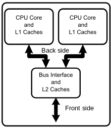
Pentium D is a range of desktop 64-bit x86-64 processors based on the NetBurst microarchitecture, which is the dual-core variant of the Pentium 4 manufactured by Intel. Each CPU comprised two cores. The brand's first processor, codenamed Smithfield and manufactured on the 90 nm process, was released on May 25, 2005, followed by the 65 nm Presler nine months later. The core implementation on the 90 nm "Smithfield" and later 65 nm "Presler" are designed differently but are functionally the same. The 90 nm "Smithfield" contains a single die, with two adjoined but functionally separate CPU cores cut from the same wafer. The later 65 nm "Presler" utilized a multi-chip module package, where two discrete dies each containing a single core reside on the CPU substrate. Neither the 90nm "Smithfield" nor the 65 nm "Presler" were capable of direct core to core communication, relying instead on the northbridge link to send information between the 2 cores.

The Intel QuickPath Interconnect (QPI) is a point-to-point processor interconnect developed by Intel which replaced the front-side bus (FSB) in Xeon, Itanium, and certain desktop platforms starting in 2008. It increased the scalability and available bandwidth. Prior to the name's announcement, Intel referred to it as Common System Interface (CSI). Earlier incarnations were known as Yet Another Protocol (YAP) and YAP+.

<span class="mw-page-title-main">CPU multiplier</span> Mechanism that sets the ratio of an internal CPU clock rate to the externally supplied clock

In computing, the clock multiplier sets the ratio of an internal CPU clock rate to the externally supplied clock. This may be implemented with phase-locked loop (PLL) frequency multiplier circuitry. A CPU with a 10x multiplier will thus see 10 internal cycles for every external clock cycle. For example, a system with an external clock of 100 MHz and a 36x clock multiplier will have an internal CPU clock of 3.6 GHz. The external address and data buses of the CPU also use the external clock as a fundamental timing base; however, they could also employ a (small) multiple of this base frequency to transfer data faster.

<span class="mw-page-title-main">Pumping (computer systems)</span>

Pumping, when referring to computer systems, is an informal term for transmitting a data signal more than one time per clock signal.

The AMD 700 chipset series is a set of chipsets designed by ATI for AMD Phenom processors to be sold under the AMD brand. Several members were launched in the end of 2007 and the first half of 2008, others launched throughout the rest of 2008.

<span class="mw-page-title-main">Quad data rate</span>

Quad data rate is a communication signaling technique wherein data are transmitted at four points in the clock cycle: on the rising and falling edges, and at two intermediate points between them. The intermediate points are defined by a second clock that is 90° out of phase from the first. The effect is to deliver four bits of data per signal line per clock cycle.

Coherent Accelerator Processor Interface (CAPI), is a high-speed processor expansion bus standard for use in large data center computers, initially designed to be layered on top of PCI Express, for directly connecting central processing units (CPUs) to external accelerators like graphics processing units (GPUs), ASICs, FPGAs or fast storage. It offers low latency, high speed, direct memory access connectivity between devices of different instruction set architectures.

References

  1. Scott Mueller (2003). Upgrading and repairing PCs (15th ed.). Que Publishing. p.  314. ISBN   978-0-7897-2974-3.
  2. Todd Langley and Rob Kowalczyk (January 2009). "Introduction to Intel Architecture: The Basics" (PDF). "White paper". Intel Corporation. Archived from the original (PDF) on June 7, 2011. Retrieved May 28, 2011.
  3. Charlie Demerjian (April 17, 2007). "Intel opens up its front side bus to the world+dog: IDF Spring 007 Xilinx heralds the bombshell". The Inquirer. Archived from the original on October 7, 2012. Retrieved May 28, 2011.{{cite news}}: CS1 maint: unfit URL (link)
  4. "Nallatech Launches Early Access Program for the Industry's First FSB-FPGA Module". Business Wire news release. Nallatech. September 18, 2007. Retrieved June 14, 2011.
  5. "XtremeData Offers Stratix III FPGA-Based Intel FSB Module". Business Wire news release. Chip Design magazine. September 18, 2007. Archived from the original on July 23, 2011. Retrieved June 14, 2011.
  6. Ashlee Vance (April 17, 2007). "High fiber diet gives Intel 'regularity' needed to beat AMD". The Register. Retrieved May 28, 2011.
  7. "XtremeData Begins Shipping 1066 MHz Altera Stratix III FPGA-Based Intel FSB Module". Business Wire news release. XtremeData. June 17, 2008. Retrieved June 14, 2011.
  8. Allan McNaughton (September 29, 2003). "AMD HyperTransport Bus: Transport Your Application to Hyper Performance". AMD. Archived from the original on March 25, 2012. Retrieved June 14, 2011.
  9. "An Introduction to the Intel QuickPath Interconnect" (PDF). Intel Corporation. January 30, 2009. Retrieved June 14, 2011.