Haswell (microarchitecture)

Last updated
Haswell
Haswell Chip.jpg
A Haswell wafer with several dies, with a pin for scale
General information
LaunchedJune 4, 2013;10 years ago (June 4, 2013)
Marketed by Intel
Designed byIntel
Common manufacturer(s)
  • Intel
CPUID code0306C3h
Product code
Performance
Max. CPU clock rate 800 MHz to 4.4 GHz
QPI speeds9.6 GT/s
DMI speeds4 GT/s
Cache
L1 cache 64  KB per core (32 KB instructions + 32 KB data)
L2 cache256 KB per core
L3 cache2–45  MB (shared)
L4 cache128 MB of eDRAM (Iris Pro models only)
Architecture and classification
Technology node 22 nm (Tri-Gate)
Microarchitecture Haswell
Instruction set x86-16, IA-32, x86-64
Extensions
Physical specifications
Cores
    • 2–4 (mainstream)
    • 6–8 (enthusiast)
    • 2–18 (Xeon)
GPU(s)
  • HD Graphics 4200
  • HD Graphics 4400
  • HD Graphics 4600
  • HD Graphics 5000
  • Iris 5100
  • Iris Pro 5200
Socket(s)
Products, models, variants
Model(s)
  • Haswell-DT
  • Haswell-ULT
  • Haswell-ULX
  • Haswell-H
  • Haswell-MB
  • Haswell-E
  • Haswell-EP
  • Haswell-EX
Brand name(s)
    • Core i3
    • Core i5
    • Core i7
    • Xeon E3 v3
    • Xeon E5 v3
    • Xeon E7 v3
    • Pentium
    • Celeron
History
Predecessor(s) Sandy Bridge (Tock)
Ivy Bridge (Tick)
Successor(s) Broadwell (Tick/Process)
Skylake (Tock)
Support status
Unsupported

Haswell is the codename for a processor microarchitecture developed by Intel as the "fourth-generation core" successor to the Ivy Bridge (which is a die shrink/tick of the Sandy Bridge microarchitecture). [1] Intel officially announced CPUs based on this microarchitecture on June 4, 2013, at Computex Taipei 2013, [2] while a working Haswell chip was demonstrated at the 2011 Intel Developer Forum. [3] Haswell was the last generation of Intel processor to have socketed processors on mobile. With Haswell, which uses a 22 nm process, [4] Intel also introduced low-power processors designed for convertible or "hybrid" ultrabooks, designated by the "U" suffix. Haswell began shipping to manufacturers and OEMs in mid-2013, with its desktop chips officially launched in September 2013.

Contents

Haswell CPUs are used in conjunction with the Intel 8 Series chipsets, 9 Series chipsets, and C220 series chipsets.

At least one Haswell-based processor was still being sold in 2022the Pentium G3420. [5] [6] Windows 7 through Windows 10 were released for the Haswell microarchitecture.

Design

The Haswell architecture is specifically designed [7] to optimize the power savings and performance benefits from the move to FinFET (non-planar, "3D") transistors on the improved 22 nm process node. [8]

Haswell has been launched in three major forms: [9]

Notes

Performance

Compared to Ivy Bridge:

Technology

Features carried over from Ivy Bridge

New features

Haswell featured a Fully Integrated Voltage Regulator. Fully Integrated Voltage Regulator.svg
Haswell featured a Fully Integrated Voltage Regulator.

CPU

Translation lookaside buffer sizes [44] [45]
CachePage size
NameLevel4 KB2 MB1 GB
DTLB1st64324
ITLB1st1288 / logical corenone
STLB2nd1024none

GPU

  • Hardware graphics support for Direct3D 11.1 and OpenGL 4.3. [46] [47] [48] Intel 10.18.14.5180 driver is the last planned driver release on Windows 7/8.1. [49]
  • Four versions of the integrated GPU: GT1, GT2, GT3 and GT3e, where GT3 version has 40 execution units (EUs). Haswell's predecessor, Ivy Bridge, has a maximum of 16 EUs. GT3e version with 40 EUs and on-package 128 MB of embedded DRAM (eDRAM), called Crystalwell, is available only in mobile H-SKUs and desktop (BGA-only) R-SKUs. Effectively, this eDRAM is a Level 4 cache; it is shared dynamically between the on-die GPU and CPU, and serving as a victim cache to the CPU's Level 3 cache. [50] [51] [52] [53] [54]

I/O

Server processors features

Haswell Refresh

Around the middle of 2014, Intel released a refresh of Haswell, simply titled Haswell Refresh. When compared to the original Haswell CPUs lineup, Haswell Refresh CPUs offer a modest increase in clock frequencies, usually of 100 MHz. [77] Haswell Refresh CPUs are supported by Intel's 9 Series chipsets (Z97 and H97, codenamed Wildcat Point), while motherboards with 8 Series chipsets (codenamed Lynx Point) usually require a BIOS update to support Haswell Refresh CPUs. [78]

The CPUs codenamed Devil's Canyon, covering the i5 and i7 K-series SKUs, employ a new and improved thermal interface material (TIM) called next-generation polymer thermal interface material (NGPTIM). This improved TIM reduces the CPU's operating temperatures and improves the overclocking potential, as something that had been problematic since the introduction of Ivy Bridge. [79] Other changes for the Devil's Canyon CPUs include a TDP increase to 88 W, additional decoupling capacitors to help smooth out the outputs from the fully integrated voltage regulator (FIVR), and support for the VT-d that was previously limited to non-K-series SKUs. [80] TSX was another feature brought over from the non-K-series SKUs, until August 2014 when a microcode update disabled TSX due to a bug that was discovered in its implementation. [35] [36]

Windows XP and Vista support

While Ivy Bridge is the last Intel processor to fully support all versions of Windows XP, Haswell includes limited driver support for certain XP editions such as POSReady2009. People have modified the graphics driver for these versions to adapt to normal Windows XP to varying degrees of success.

Windows Vista support is also dropped with this processor as well. People who have installed x64 version of Vista have reported various problems such as services not starting automatically. The KB4493471 update (officially intended only for Windows Server 2008, but can be installed on Vista) contains a HAL driver that allegedly fixes these issues; however, upon several tests it's been confirmed - it doesn't fix any of the issues. Windows XP and earlier, and all x86 versions and editions of Vista are unaffected by this bug.[ citation needed ]

List of Haswell processors

Desktop processors

Intel Haswell i7-4771 CPU, sitting atop its original packaging that contains an OEM fan-cooled heatsink Intel Haswell 4771 CPU.jpg
Intel Haswell i7-4771 CPU, sitting atop its original packaging that contains an OEM fan-cooled heatsink

The following table lists available desktop processors.

Target
segment
Cores
(threads)
Processor
branding and model
GPU modelCPU clock rate GPU clock rate Cache TDP PCIe 3.0 lane
configurations [a]
VT-d [b] Release
date
Release
price
(USD)
Motherboard
Base Turbo BaseTurbo L3 L4 [lower-alpha 1] SocketInterfaceMemory
Enthusiast / High-End8 (16)Core i7
Extreme
5960X 3.0 GHz3.5 GHz20 MB140 W2×16 + 1×8YesAugust 29, 2014 [89] $999 LGA 2011-v3 DMI 2.0
PCIe 3.0
Up to quad
channel
DDR4-2133
6 (12) 5930K 3.5 GHz3.7 GHz15 MB$583
5820K 3.3 GHz3.6 GHz1×16 + 1×8 + 1×4$389
Performance4 (8)Core i7 4790K HD 4600 
(GT2)
4.0 GHz4.4 GHz350 MHz [90] 1.25 GHz8 MB88 W1×16
2×8
1×8 + 2×4
June 2, 2014$339 LGA
1150
Up to dual
channel
DDR3-1600 [91]
4790 3.6 GHz4.0 GHz1.2 GHz84 WMay 11, 2014$303
4790S 3.2 GHz65 W
4790T 2.7 GHz3.9 GHz45 W
4785T 2.2 GHz3.2 GHz35 W
4771 3.5 GHz3.9 GHz84 WSeptember 1, 2013$320
4770K 1.25 GHzNoJune 2, 2013 [92] $339
4770 3.4 GHz1.2 GHzYes$303
4770S 3.1 GHz65 W
4770R Iris Pro 5200 
(GT3e)
3.2 GHz200 MHz1.3 GHz6 MB128 MB$392BGA
1364
4770T HD 4600 
(GT2)
2.5 GHz3.7 GHz350 MHz [90] 1.2 GHz8 MB45 W$303 LGA
1150
4770TE 2.3 GHz3.3 GHz1 GHz
4765T 2.0 GHz3.0 GHz1.2 GHz35 W
Mainstream4 (4)Core i5 4690K 3.5 GHz3.9 GHz6 MB88 WJune 2, 2014$242
4690 84 WMay 11, 2014$213
4690S 3.2 GHz65 W
4690T 2.5 GHz3.5 GHz45 W
4670K 3.4 GHz3.8 GHz84 WNoJune 2, 2013$242
4670 Yes$213
4670S 3.1 GHz65 W
4670R Iris Pro 5200 
(GT3e)
3.0 GHz3.7 GHz200 MHz1.3 GHz4 MB128 MB$310BGA
1364
4670T HD 4600 
(GT2)
2.3 GHz3.3 GHz350 MHz [90] 1.2 GHz6 MB45 W$213 LGA
1150
4590 3.3 GHz3.7 GHz1.15 GHz84 WMay 11, 2014$192
4590S 3.0 GHz65 W
4590T 2.0 GHz3.0 GHz35 W
4570 3.2 GHz3.6 GHz84 WJune 2, 2013
4570S 2.9 GHz65 W
4570R Iris Pro 5200 
(GT3e)
2.7 GHz3.2 GHz200 MHz4 MB128 MB$288BGA
1364
2 (4) 4570T HD 4600 
(GT2)
2.9 GHz3.6 GHz35 W$192 LGA
1150
4570TE 2.7 GHz3.3 GHz350 MHz [90] 1 GHz
4 (4) 4460 3.2 GHz3.4 GHz1.1 GHz6 MB84 WMay 11, 2014$182
4460S 2.9 GHz65 W
4460T 1.9 GHz2.7 GHz35 W
4440 3.1 GHz3.3 GHz84 WSeptember 1, 2013
4440S 2.8 GHz65 W
4430 3.0 GHz3.2 GHz84 WJune 2, 2013 [92]
4430S 2.7 GHz65 W
2 (4)Core i3 4370 3.8 GHz1.15 GHz4 MB54 WNoJuly 20, 2014$149
4360 3.7 GHzMay 11, 2014
4350 3.6 GHz$138
4340 September 1, 2013$149
4330 3.5 GHz$138
4370T 3.3 GHz200 MHz35 WMarch 30, 2015
4360T 3.2 GHzJuly 20, 2014
4350T 3.1 GHzMay 11, 2014
4330T 3.0 GHzSeptember 1, 2013
4340TE 2.6 GHz350 MHz1 GHzMay 11, 2014$138
4330TE 2.4 GHzSeptember 1, 2013$122
4170 HD 4400 
(GT2)
3.7 GHz1.15 GHz3 MB54 WMarch 30, 2015$117
4160 3.6 GHzJuly 20, 2014
4150 3.5 GHzMay 11, 2014
4130 3.4 GHzSeptember 1, 2013$122
4170T 3.2 GHz200 MHz35 WMarch 30, 2015$117
4160T 3.1 GHzJuly 20, 2014
4150T 3.0 GHzMay 11, 2014
4130T 2.9 GHzSeptember 1, 2013$122
Budget2 (2)Pentium G3470 HD Graphics (GT1)3.6 GHz350 MHz1.1 GHz53 WMarch 30, 2015$86
G3460 3.5 GHzJuly 20, 2014
G3450 3.4 GHzMay 11, 2014
G3440 3.3 GHz$75
G3430 December 1, 2013$86
G3420 3.2 GHz$75
G3460T 3.0 GHz200 MHz1.1 GHz35 WMarch 30, 2015
G3450T 2.9 GHzJuly 20, 2014
G3440T 2.8 GHzMay 11, 2014
G3420T 2.7 GHzDecember 1, 2013
G3320TE 2.3 GHz350 MHz1 GHzUp to dual
channel
DDR3-1333
G3260 3.3 GHz1.1 GHz53 WMarch 30, 2015$64
G3258 [c] 3.2 GHzJune 2, 2014$72
G3250 July 20, 2014$64
G3240 3.1 GHzMay 11, 2014
G3220 3.0 GHzDecember 1, 2013
G3260T 2.9 GHz200 MHz35 WMarch 30, 2015
G3250T 2.8 GHzJuly 20, 2014
G3240T 2.7 GHzMay 11, 2014
G3220T 2.6 GHzDecember 1, 2013
Celeron G1850 2.9 GHz350 MHz1.05 GHz2 MB53 WMay 11, 2014$52
G1840 2.8 GHz$42
G1830 December 1, 2013$52
G1820 2.7 GHz$42
G1840T 2.5 GHz200 MHz35 WMay 11, 2014
G1820T 2.4 GHzDecember 1, 2013
G1820TE 2.2 GHz1 GHz
a Some of these configurations could be disabled by the chipset. For example, H-series chipsets disable all PCIe 3.0 lane configurations except 1×16.
b This feature also requires a chipset that supports VT-d like the Q87 chipset or the X99 chipset.
c This is called 20th Anniversary Edition and has an unlocked multiplier.

SKU suffixes to denote:

Server processors

Intel Xeon E3-1241 v3 CPU.jpg
Intel Xeon E3-1241 v3 CPU, on top of its original packaging with an OEM fan-cooled heatsink
Intel Xeon E5-1650 v3 CPU.jpg
Intel Xeon E5-1650 v3 CPU; its retail box contains no OEM heatsink

The first digit of the model number designates the largest supported multi-socket configuration; thus, E5-26xx v3 models support up to dual-socket configurations, while the E7-48xx v3 and E7-88xx v3 models support up to quad- and eight-socket configurations, respectively. Also, E5-16xx/26xx v3 and E7-48xx/88xx v3 models have no integrated GPU.

Lists of launched server processors are below, split between Haswell E3-12xx v3, E5-16xx/26xx v3 and E7-48xx/88xx v3 models.

Haswell E7-48xx/88xx v3 SKUs [94] [95]
Target
segment
Cores
(threads)
Processor
branding and model
CPU clock rate L3
cache
TDP Release
date
Release
price
(USD)
Motherboard
Normal Turbo SocketInterfaceMemory
Server4 (8) Xeon E7 v3 E7-8893v3 3.2 GHz3.5 GHz45 MB140 WMay 2015$6,841 LGA
2011-1
QPI (up to
9.6 GT/s [lower-alpha 2] )
DMI 2.0
PCIe 3.0
Up to DDR4-1866 or DDR3-1600
10 (20) E7-8891v3 2.8 GHz165 W
18 (36) E7-8890v3 2.5 GHz3.3 GHz$7,174
E7-8880v3 2.3 GHz3.1 GHz150 W$5,895
E7-8880Lv3 2.0 GHz2.8 GHz115 W$6,063
E7-8870v3 2.1 GHz2.9 GHz140 W$4,672
16 (32) E7-8867v3 2.5 GHz3.3 GHz165 W
E7-8860v3 2.2 GHz3.2 GHz40 MB$4,061
14 (28) E7-4850v3 2.8 GHz35 MB115 W$3,003
12 (24) E7-4830v3 2.1 GHz2.7 GHz30 MB$2,170
10 (20) E7-4820v3 1.9 GHz25 MB$1,502
8 (16) E7-4809v3 2.0 GHz
Haswell E5-16xx/26xx v3 SKUs
Target
segment
Cores
(threads)
Processor
branding and model
CPU clock rate CPU
AVX clock rate [96]
L3
cache
TDP Release
date
Release
price
(USD)
tray / box
Motherboard
Normal Turbo NormalTurboSocketInterfaceMemory
Server18 (36) Xeon E5 v3 2699v3 2.3 GHz3.6 GHz1.9 GHz3.3 GHz45 MB145 WSeptember 9, 2014 LGA
2011-3
QPI (up to
9.6 GT/s [lower-alpha 2] )
DMI 2.0
PCIe 3.0
up to DDR4-2133
16 (32) 2698v3 40 MB135 W
2698Av3 [97] 2.8 GHz3.2 GHz2.3 GHz2.9 GHz165 WNovember 2014OEM
14 (28) 2697v3 2.6 GHz3.6 GHz2.2 GHz3.3 GHz35 MB145 WSeptember 9, 2014$2,702 / $2,706
2695v3 2.3 GHz3.3 GHz1.9 GHz3.0 GHz120 W$2,424 / $2,428
12 (24) 2690v3 2.6 GHz3.5 GHz2.3 GHz3.2 GHz30 MB135 W$2,090 / $2,094
14 (28) 2683v3 2.0 GHz3.0 GHz1.7 GHz2.7 GHz35 MB120 W$1,846 / 
12 (24) 2680v3 2.5 GHz3.3 GHz2.1 GHz3.1 GHz30 MB$1,745 / $1,749
2673v3 [lower-alpha 3] 2.4 GHz3.1 GHz105 W
2670v3 2.3 GHz3.1 GHz2.0 GHz2.9 GHz120 W$1,589 / $1,593
8 (16) 2667v3 3.2 GHz3.6 GHz2.7 GHz3.5 GHz20 MB135 W$2,057 / 
10 (20) 2660v3 2.6 GHz3.3 GHz2.2 GHz3.1 GHz25 MB105 W$1,445 / $1,449
12 (24) 2650Lv3 1.8 GHz2.5 GHz1.5 GHz2.3 GHz30 MB65 W$1,329 / 
2658v3 2.2 GHz2.9 GHz1.9 GHz3.0 GHz105 W$1,832 / 
10 (20) 2650v3 2.3 GHz3.0 GHz2.0 GHz2.8 GHz25 MB$1,166 / $1,171
12 (24) 2648Lv3 1.8 GHz2.5 GHz1.5 GHz2.2 GHz30 MB75 W$1,544 / 
6 (12) 2643v3 3.4 GHz3.7 GHz2.8 GHz3.6 GHz20 MB135 W$1,552 / 
8 (16) 2640v3 2.6 GHz3.4 GHz2.2 GHz3.4 GHz20 MB90 W$939 / $944up to DDR4-1866
4 (8) 2637v3 3.5 GHz3.7 GHz3.2 GHz3.6 GHz15 MB135 W$996 / up to DDR4-2133
8 (16) 2630v3 2.4 GHz3.2 GHz2.1 GHz3.2 GHz20 MB85 W$667 / $671up to DDR4-1866
2630Lv3 1.8 GHz2.9 GHz1.5 GHz2.9 GHz55 W$612 / 
10 (20) 2628Lv3 2.0 GHz2.5 GHz1.7 GHz2.4 GHz25 MB75 W$1,364 / 
4 (8) 2623v3 3.0 GHz3.5 GHz2.7 GHz3.5 GHz10 MB105 W$444 / 
6 (12) 2620v3 2.4 GHz3.2 GHz2.1 GHz3.2 GHz15 MB85 W$417 / $422
8 (16) 2618Lv3 2.3 GHz3.4 GHz1.9 GHz3.4 GHz20 MB75 W$779 / 
6 (6) 2609v3 1.9 GHz1.9 GHz15 MB85 W$306 / $306up to DDR4-1600
6 (12) 2608Lv3 2.0 GHz1.7 GHz52 W$441 / up to DDR4-1866
6 (6) 2603v3 1.6 GHz1.3 GHz85 W$213 / $217up to DDR4-1600
Workstation10 (20) 2687Wv3 3.1 GHz3.5 GHz2.7 GHz3.5 GHz25 MB160 W$2,141 / $2,145up to DDR4-2133
8 (16) 1680v3 3.2 GHz3.8 GHz2.9 GHz3.4 GHz20 MB140 W$1,723 /  DMI 2.0
PCIe 3.0
1660v3 3.0 GHz3.5 GHz2.7 GHz3.5 GHz$1,080 / 
6 (12) 1650v3 3.5 GHz3.8 GHz3.2 GHz3.7 GHz15 MB$583 / $586
4 (8) 1630v3 3.7 GHz3.8 GHz3.4 GHz3.7 GHz10 MB$372 / 
1620v3 3.5 GHz3.6 GHz3.2 GHz3.5 GHz$294 / $297
4 (4) 1607v3 3.1 GHz2.8 GHz$255 / —up to DDR4-1866
4 (4) 1603v3 2.8 GHz2.5 GHz$202 / —
Haswell E3-12xx v3 SKUs
Target
segment
Cores
(threads)
Processor
branding and model
GPU modelCPU clock rate Graphics clock rate L3
cache
GPU
eDRAM
TDP Release
date
Release
price
(USD)
tray / box
Motherboard
Normal Turbo NormalTurboSocketInterfaceMemory
Server4 (8) Xeon E3 v3 1286v3 HD P4700 (GT2)3.7 GHz4.1 GHz350 MHz1.3 GHz8 MB84 WMay 11, 2014$662 /  LGA
1150
DMI 2.0
PCIe 3.0
up to dual
channel
DDR3-1600
with ECC
1286Lv3 3.2 GHz4.0 GHz1.25 GHz65 W$774 / 
1285v3 3.6 GHz1.3 GHz84 WJune 2, 2013$662 / 
1285Lv3 3.1 GHz3.9 GHz1.25 GHz65 W$774 / 
1284Lv3 Iris Pro 5200 (GT3e)1.8 GHz3.2 GHz750 MHz1 GHz6 MB128 MB47 WFebruary 18, 2014OEMBGA
1364
1281v3 3.7 GHz4.1 GHz8 MB82 WMay 11, 2014$612 /  LGA
1150
1280v3 3.6 GHz4.0 GHzJune 2, 2013
1276v3 HD P4600 (GT2)350 MHz1.25 GHz84 WMay 11, 2014$339 / $350
1275v3 3.5 GHz3.9 GHzJune 2, 2013$339 / $350
1275Lv3 HD (GT1)2.7 GHz1.2 GHz45 WMay 11, 2014$328 / 
1271v3 3.6 GHz4.0 GHz80 W$328 / $339
1270v3 3.5 GHz3.9 GHzJune 2, 2013
1268Lv3 HD P4600 (GT2)2.3 GHz3.3 GHz350 MHz1 GHz45 W$310 / 
1265Lv3 HD (GT1)2.5 GHz3.7 GHz1.2 GHz$294 / 
1246v3 HD P4600 (GT2)3.5 GHz3.9 GHz84 WMay 11, 2014$276 / $287
1245v3 3.4 GHz3.8 GHzJune 2, 2013
1241v3 3.5 GHz3.9 GHz80 WMay 11, 2014$262 / $273
1240v3 3.4 GHz3.8 GHzJune 2, 2013
1240Lv3 2.0 GHz3.0 GHz25 WMay 11, 2014$278 / 
1231v3 3.4 GHz3.8 GHz80 W$240 / $250
1230v3 3.3 GHz3.7 GHzJune 2, 2013
1230Lv3 1.8 GHz2.8 GHz25 W$250 / 
4 (4) 1226v3 HD P4600 (GT2)3.3 GHz3.7 GHz350 MHz1.2 GHz84 WMay 11, 2014$213 / $224
1225v3 3.2 GHz3.6 GHzJune 2, 2013
1220v3 3.1 GHz3.5 GHz80 W$193 / $203
2 (4) 1220Lv3 1.1 GHz1.5 GHz4 MB13 WSeptember 1, 2013$193 / 

SKU suffixes to denote:

Mobile processors

The following table lists available mobile processors.

Target
segment
Cores
(threads)
Processor
branding and model
GPU model Programmable TDP [101] :69–72CPU Turbo
(single core)
GPU clock rate L3
cache
GPU eDRAM Release
date
Release
price
(USD)
SDP [102] [103] :71 cTDP down [a] Nominal TDP [b] cTDP up [c] BaseTurbo
Performance 4 (8) Core i7 4940MX HD 4600 (GT2)57 W / 3.1 GHz65 W / 3.8 GHz 4.0 GHz400 MHz1.35 GHz8 MBJanuary 21, 2014 [104] $1096
4930MX 57 W / 3.0 GHz65 W / 3.7 GHz 3.9 GHzJune 2, 2013 [105]
4980HQ Iris Pro 5200 (GT3e)47 W / 2.8 GHz 4.0 GHz200 MHz1.3 GHz6 MB128 MB [51] July 21, 2014 [106] $623
4960HQ 47 W / 2.6 GHz55 W / 3.6 GHz 3.8 GHzSeptember 1, 2013 [107]
4950HQ 47 W / 2.4 GHz55 W / 3.4 GHz 3.6 GHzJune 2, 2013 [105]
4910MQ HD 4600 (GT2)47 W / 2.9 GHz55 W / 3.7 GHz 3.9 GHz400 MHz8 MBJanuary 21, 2014 [104] $568
4900MQ 47 W / 2.8 GHz55 W / 3.6 GHz 3.8 GHzJune 2, 2013 [105] $570
4870HQ Iris Pro 5200 (GT3e)47 W / 2.5 GHz 3.7 GHz200 MHz1.2 GHz6 MB128 MBJuly 21, 2014 [106] $434
4860EQ 47 W / 1.8 GHz 3.2 GHz750 MHz1 GHzAugust 2013$508
4860HQ 47 W / 2.4 GHz55 W / 3.4 GHz 3.6 GHz200 MHz1.2 GHzJanuary 21, 2014 [104] $434
4850EQ 47 W / 1.6 GHz 3.2 GHz650 MHz1 GHzAugust 2013$466
4850HQ 47 W / 2.3 GHz55 W / 3.3 GHz 3.5 GHz200 MHz1.2 GHzJune 2, 2013 [105] $434
4810MQ HD 4600 (GT2)47 W / 2.8 GHz55 W / 3.6 GHz 3.8 GHz400 MHz1.3 GHzJanuary 21, 2014 [104] $378
4800MQ 47 W / 2.7 GHz55 W / 3.5 GHz 3.7 GHzJune 2, 2013 [105] $380
4770HQ Iris Pro 5200 (GT3e)47 W / 2.2 GHz 3.4 GHz200 MHz1.2 GHz128 MBJuly 21, 2014 [106] $434
4760HQ 47 W / 2.1 GHz55 W / 3.1 GHz 3.3 GHzApril 14, 2014$434
4750HQ 47 W / 2.0 GHz55 W / 3.0 GHz 3.2 GHzJune 2, 2013 [105] $440
4720HQ HD 4600 (GT2)47 W / 2.6 GHz 3.6 GHz400 MHz1.2 GHzJanuary 2015$378
4712MQ 37 W / 2.3 GHz45 W / 3.1 GHz 3.3 GHz1.15 GHzApril 14, 2014
4712HQ
4710MQ 47 W / 2.5 GHz55 W / 3.3 GHz 3.5 GHz
4710HQ 1.2 GHz
4702MQ 37 W / 2.2 GHz45 W / 2.9 GHz 3.2 GHz1.15 GHzJune 2, 2013 [105] $383
4702HQ
4700MQ 47 W / 2.4 GHz55 W / 3.2 GHz 3.4 GHz
4700HQ 1.2 GHz
4701EQ 1 GHzSeptember 1, 2013$415
4700EQ June 2, 2013 [105] $378
4702EC 27 W / 2.0 GHz8 MBApril 2014$459
4700EC 43 W / 2.7 GHz
Mainstream 2 (4) 4650U HD 5000 (GT3)11.5 W / 800 MHz15 W / 1.7 GHz 3.3 GHz200 MHz1.1 GHz4 MBJune 2, 2013 [105] $454
4610Y HD 4200 (GT2)6 W / 800 MHz9.5 W / 800 MHz11.5 W / 1.7 GHz 2.9 GHz850 MHzSeptember 1, 2013$393
4610M HD 4600 (GT2)37 W / 3.0 GHz 3.7 GHz400 MHz1.3 GHzJanuary 21, 2014 [104] $346
4600M 37 W / 2.9 GHz 3.6 GHzSeptember 1, 2013
4600U HD 4400 (GT2)11.5 W / 800 MHz15 W / 2.1 GHz 3.3 GHz200 MHz1.1 GHz$398
4578U Iris 5100 (GT3)23 W / 800 MHz28 W / 3.0 GHz 3.5 GHz1.2 GHzJuly 20, 2014
4558U 28 W / 2.8 GHz 3.3 GHz1.2 GHzJune 2, 2013 [105] $454
4550U HD 5000 (GT3)11.5 W / 800 MHz15 W / 1.5 GHz 3.0 GHz1.1 GHz
4510U HD 4400 (GT2)15 W / 2.0 GHz 3.1 GHzApril 2014$393
4500U 15 W / 1.8 GHz25 W / 3.0 GHz 3.0 GHzJune 2, 2013 [105] $398
 Core i5 4402EC 27 W / 2.5 GHzApril 2014$324
4422E HD 4600 (GT2)25 W / 1.8 GHz 2.9 GHz400 MHz900 MHz3 MBApril 14, 2014$266
4410E 37 W / 2.9 GHz1 GHz
4402E 25 W / 1.6 GHz 2.7 GHz900 MHzSeptember 1, 2013
4400E 37 W / 2.7 GHz 3.3 GHz1 GHz
4360U HD 5000 (GT3)11.5 W / 800 MHz15 W / 1.5 GHz 3.0 GHz200 MHz1.1 GHzJanuary 21, 2014 [104] $315
4350U 15 W / 1.4 GHz 2.9 GHzJune 2, 2013 [105] $342
4340M HD 4600 (GT2)37 W / 2.9 GHz 3.6 GHz400 MHz1.25 GHzJanuary 21, 2014 [104] $266
4330M 37 W / 2.8 GHz 3.5 GHzSeptember 1, 2013
4310M HD 4600 (GT2)37 W / 2.7 GHz 3.4 GHz400 MHz1.25 GHzJanuary 21, 2014 [104] $225
4310U HD 4400 (GT2)11.5 W / 800 MHz15 W / 2.0 GHz 3.0 GHz200 MHz1.1 GHz$281
4302Y HD 4200 (GT2)4.5 W / 800 MHz11.5 W / 1.6 GHz 2.3 GHz200 MHz850 MHzSeptember 1, 2013
4300Y 6 W / 800 MHz9.5 W / 800 MHz$304
4300M HD 4600 (GT2)37 W / 2.6 GHz 3.3 GHz400 MHz1.25 GHz$225
4300U HD 4400 (GT2)11.5 W / 800 MHz15 W / 1.9 GHz 2.9 GHz200 MHz1.1 GHz$287
4288U Iris 5100 (GT3)23 W / 800 MHz28 W / 2.6 GHz 3.1 GHz1.2 GHzJune 2, 2013 [105] $342
4258U 28 W / 2.4 GHz 2.9 GHz1.1 GHz
4308U 28 W / 2.8 GHz 3.3 GHz1.2 GHzJuly 20, 2014 [108] $315
4260U HD 5000 (GT3)11.5 W / 800 MHz15 W / 1.4 GHz 2.7 GHz1 GHzApril 14, 2014$315
4250U 15 W / 1.3 GHz 2.6 GHzJune 2, 2013 [105] $342
4210H HD 4600 (GT2)47 W / 2.9 GHz 3.5 GHz400 MHz1.15 GHzJuly 20, 2014$225
4210M 37 W / 2.6 GHz 3.2 GHzApril 14, 2014
4210U HD 4400 (GT2)11.5 W / 800 MHz15 W / 1.7 GHz 2.7 GHz200 MHz1 GHz$287
4220Y HD 4200 (GT2)6 W / 800 MHz9.5 W / 800 MHz11.5 W / 1.6 GHz 2.0 GHz850 MHz$281
4210Y 11.5 W / 1.5 GHz 1.9 GHzSeptember 1, 2013$304
4202Y 4.5 W / 800 MHz11.5 W / 1.6 GHz 2.0 GHz
4200Y 6 W / 800 MHz11.5 W / 1.4 GHz 1.9 GHzJune 2, 2013 [105] $304
4200U HD 4400 (GT2)11.5 W / 800 MHz15 W / 1.6 GHz25 W / ? 2.6 GHz1 GHz$287
4200H HD 4600 (GT2)47 W / 2.8 GHz 3.4 GHz400 MHz1.15 GHzSeptember 1, 2013$257
4200M 37 W / 2.5 GHz 3.1 GHz$240
 Core i3 4158U Iris 5100 (GT3)23 W / 800 MHz28 W / 2.0 GHz200 MHz1.1 GHzJune 2, 2013 [105] $342
4120U HD 4400 (GT2)11.5 W / 800 MHz15 W / 2.0 GHz1 GHzApril 14, 2014$281
4112E HD 4600 (GT2)25 W / 1.8 GHz400 MHz900 MHz$225
4110E 37 W / 2.6 GHz
4102E 25 W / 1.6 GHzSeptember 1, 2013
4100E 37 W / 2.4 GHz
4110M 37 W / 2.6 GHz1.1 GHzApril 14, 2014
4100M 37 W / 2.5 GHzSeptember 1, 2013
4100U HD 4400 (GT2)11.5 W / 800 MHz15 W / 1.8 GHz200 MHz1 GHzJune 2, 2013 [105] $287
4030Y HD 4200 (GT2)6 W / 800 MHz9.5 W / 800 MHz11.5 W / 1.6 GHz850 MHzApril 14, 2014$281
4020Y 11.5 W / 1.5 GHzSeptember 1, 2013$304
4012Y 4.5 W / 800 MHz
4010Y 6 W / 800 MHz9.5 W / 800 MHz11.5 W / 1.3 GHzJune 2, 2013 [105]
4030U HD 4400 (GT2)11.5 W / 800 MHz15 W / 1.9 GHz1 GHzApril 14, 2014$281
4025U 950 MHz$275
4010U 15 W / 1.7 GHz1 GHzSeptember 1, 2013$287
4005U 950 MHz$281
4000M HD 4600 (GT2)37 W / 2.4 GHz400 MHz1.1 GHz$240
Budget 2 (2) Pentium 3561Y HD Graphics (GT1)6 W / 800 MHz11.5 W / 1.2 GHz200 MHz850 MHz2 MBDecember 2013$161
3560Y September 1, 2013OEM
3558U 15 W / 1.7 GHz1 GHzDecember 2013$161
3556U September 1, 2013OEM
3560M 37 W / 2.4 GHz400 MHz1.1 GHzApril 14, 2014$134
3550M 37 W / 2.3 GHzSeptember 1, 2013
 Celeron 2981U 15 W / 1.6 GHz200 MHz1 GHzDecember 2013$137
2980U September 1, 2013
2957U 15 W / 1.4 GHzDecember 2013$132
2955U September 1, 2013
2970M 37 W / 2.2 GHz400 MHz1.1 GHzApril 14, 2014$75
2950M 37 W / 2.0 GHzSeptember 1, 2013$86
2961Y 6 W / 800 MHz11.5 W / 1.1 GHz200 MHz850 MHzDecember 2013OEM
  1. When a cooler or quieter mode of operation is desired, this mode specifies a lower TDP and lower guaranteed frequency versus the nominal mode. [101] :71–72
  2. This is the processor's rated frequency and TDP. [101] :71–72
  3. When extra cooling is available, this mode specifies a higher TDP and higher guaranteed frequency versus the nominal mode. [101] :71–72

SKU suffixes to denote:

See also

Notes

  1. Implemented as eDRAM and serving primarily to increase the performance of integrated GPU, while being shared with the CPU.
  2. 1 2 Maximum QPI speed depends on the CPU model.
  3. Unconfirmed details may differ from surrounding models

Related Research Articles

<span class="mw-page-title-main">Xeon</span> Line of Intel server and workstation processors

Xeon is a brand of x86 microprocessors designed, manufactured, and marketed by Intel, targeted at the non-consumer workstation, server, and embedded markets. It was introduced in June 1998. Xeon processors are based on the same architecture as regular desktop-grade CPUs, but have advanced features such as support for error correction code (ECC) memory, higher core counts, more PCI Express lanes, support for larger amounts of RAM, larger cache memory and extra provision for enterprise-grade reliability, availability and serviceability (RAS) features responsible for handling hardware exceptions through the Machine Check Architecture (MCA). They are often capable of safely continuing execution where a normal processor cannot due to these extra RAS features, depending on the type and severity of the machine-check exception (MCE). Some also support multi-socket systems with two, four, or eight sockets through use of the Ultra Path Interconnect (UPI) bus, which replaced the older QuickPath Interconnect (QPI) bus.

<span class="mw-page-title-main">Land grid array</span> Type of surface-mount packaging for integrated circuits

The land grid array (LGA) is a type of surface-mount packaging for integrated circuits (ICs) that is notable for having the pins on the socket — as opposed to pins on the integrated circuit, known as a pin grid array (PGA). An LGA can be electrically connected to a printed circuit board (PCB) either by the use of a socket or by soldering directly to the board.

<span class="mw-page-title-main">Nehalem (microarchitecture)</span> CPU microarchitecture by Intel

Nehalem is the codename for Intel's 45 nm microarchitecture released in November 2008. It was used in the first generation of the Intel Core i5 and i7 processors, and succeeds the older Core microarchitecture used on Core 2 processors. The term "Nehalem" comes from the Nehalem River.

<span class="mw-page-title-main">Sandy Bridge</span> Intel processor microarchitecture

Sandy Bridge is the codename for Intel's 32 nm microarchitecture used in the second generation of the Intel Core processors. The Sandy Bridge microarchitecture is the successor to Nehalem and Westmere microarchitecture. Intel demonstrated an A1 stepping Sandy Bridge processor in 2009 during Intel Developer Forum (IDF), and released first products based on the architecture in January 2011 under the Core brand.

<span class="mw-page-title-main">Platform Controller Hub</span> Family of Intels single-chip chipsets

The Platform Controller Hub (PCH) is a family of Intel's single-chip chipsets, first introduced in 2009. It is the successor to the Intel Hub Architecture, which used two chips–a northbridge and southbridge, and first appeared in the Intel 5 Series.

<span class="mw-page-title-main">Intel Core</span> Line of CPUs by Intel

Intel Core is a line of multi-core central processing units (CPUs) for midrange, embedded, workstation, high-end and enthusiast computer markets marketed by Intel Corporation. These processors displaced the existing mid- to high-end Pentium processors at the time of their introduction, moving the Pentium to the entry level. Identical or more capable versions of Core processors are also sold as Xeon processors for the server and workstation markets.

<span class="mw-page-title-main">LGA 2011</span> CPU socket created by Intel

LGA 2011, also called Socket R, is a CPU socket by Intel released on November 14, 2011. It launched along with LGA 1356 to replace its predecessor, LGA 1366 and LGA 1567. While LGA 1356 was designed for dual-processor or low-end servers, LGA 2011 was designed for high-end desktops and high-performance servers. The socket has 2011 protruding pins that touch contact points on the underside of the processor.

<span class="mw-page-title-main">Skylake (microarchitecture)</span> CPU microarchitecture by Intel

Skylake is Intel's codename for its sixth generation Core microprocessor family that was launched on August 5, 2015, succeeding the Broadwell microarchitecture. Skylake is a microarchitecture redesign using the same 14 nm manufacturing process technology as its predecessor, serving as a tock in Intel's tick–tock manufacturing and design model. According to Intel, the redesign brings greater CPU and GPU performance and reduced power consumption. Skylake CPUs share their microarchitecture with Kaby Lake, Coffee Lake, Whiskey Lake, and Comet Lake CPUs.

<span class="mw-page-title-main">Ivy Bridge (microarchitecture)</span> CPU microarchitecture by Intel

Ivy Bridge is the codename for Intel's 22 nm microarchitecture used in the third generation of the Intel Core processors. Ivy Bridge is a die shrink to 22 nm process based on FinFET ("3D") Tri-Gate transistors, from the former generation's 32 nm Sandy Bridge microarchitecture—also known as tick–tock model. The name is also applied more broadly to the Xeon and Core i7 Extreme Ivy Bridge-E series of processors released in 2013.

<span class="mw-page-title-main">ThinkStation</span> Line of professional workstations by Lenovo

ThinkStation is a brand of professional workstations from Lenovo announced in November 2007 and then released in January 2008. They are designed to be used for high-end computing and computer-aided design (CAD) tasks and primarily compete with other enterprise workstation lines, such as Dell's Precision, HP's Z line, Acer's Veriton K series, and Apple's Mac Pro line.

<span class="mw-page-title-main">Broadwell (microarchitecture)</span> Fifth generation of Intel Core processors

Broadwell is the fifth generation of the Intel Core processor. It is Intel's codename for the 14 nanometer die shrink of its Haswell microarchitecture. It is a "tick" in Intel's tick–tock principle as the next step in semiconductor fabrication. Like some of the previous tick-tock iterations, Broadwell did not completely replace the full range of CPUs from the previous microarchitecture (Haswell), as there were no low-end desktop CPUs based on Broadwell.

<span class="mw-page-title-main">LGA 1151</span> Intel microprocessor compatible socket

LGA 1151, also known as Socket H4, is a type of zero insertion force flip-chip land grid array (LGA) socket for Intel desktop processors which comes in two distinct versions: the first revision which supports both Intel's Skylake and Kaby Lake CPUs, and the second revision which supports Coffee Lake CPUs exclusively.

Intel X99, codenamed "Wellsburg", is a Platform Controller Hub (PCH) designed and manufactured by Intel, targeted at the high-end desktop (HEDT) and enthusiast segments of the Intel product lineup. The X99 chipset supports both Intel Core i7 Extreme and Intel Xeon E5-16xx v3 and E5-26xx v3 processors, which belong to the Haswell-E and Haswell-EP variants of the Haswell microarchitecture, respectively. All supported processors use the LGA 2011-v3 socket.

<span class="mw-page-title-main">Kaby Lake</span> Intel microprocessor, released in 2016

Kaby Lake is Intel's codename for its seventh generation Core microprocessor family announced on August 30, 2016. Like the preceding Skylake, Kaby Lake is produced using a 14 nanometer manufacturing process technology. Breaking with Intel's previous "tick–tock" manufacturing and design model, Kaby Lake represents the optimized step of the newer process–architecture–optimization model. Kaby Lake began shipping to manufacturers and OEMs in the second quarter of 2016, with its desktop chips officially launched in January 2017.

<span class="mw-page-title-main">Coffee Lake</span> Eighth-generation Intel Core microprocessor family

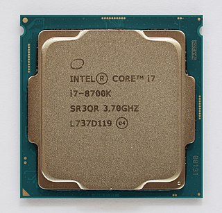
Coffee Lake is Intel's codename for its eighth-generation Core microprocessor family, announced on September 25, 2017. It is manufactured using Intel's second 14 nm process node refinement. Desktop Coffee Lake processors introduced i5 and i7 CPUs featuring six cores and Core i3 CPUs with four cores and no hyperthreading.

Comet Lake is Intel's codename for its 10th generation Core processors. They are manufactured using Intel's third 14 nm Skylake process revision, succeeding the Whiskey Lake U-series mobile processor and Coffee Lake desktop processor families. Intel announced low-power mobile Comet Lake-U CPUs on August 21, 2019, H-series mobile CPUs on April 2, 2020, desktop Comet Lake-S CPUs April 30, 2020, and Xeon W-1200 series workstation CPUs on May 13, 2020. Comet Lake processors and Ice Lake 10 nm processors are together branded as the Intel "10th Generation Core" family. Intel officially launched Comet Lake-Refresh CPUs on the same day as 11th Gen Core Rocket Lake launch. The low-power mobile Comet Lake-U Core and Celeron 5205U CPUs were discontinued on July 7, 2021.

Raptor Lake is Intel's codename for the 13th and 14th generations of Intel Core processors based on a hybrid architecture, utilizing Raptor Cove performance cores and Gracemont efficient cores. Like Alder Lake, Raptor Lake is fabricated using Intel's Intel 7 process. Raptor Lake features up to 24 cores and 32 threads and is socket compatible with Alder Lake systems. Like earlier generations, Raptor Lake processors also need accompanying chipsets.

References

  1. "Intel Developer Forum". Intel.com. Intel . Retrieved 2012-01-04.
  2. Moorhead, Patrick (4 June 2013). "Intel's Newest Core Processors: All About Graphics And Low Power". Forbes.
  3. Crothers, Brooke (2011-09-14). "Haswell chip completes Ultrabook 'revolution'". News.cnet.com. Retrieved 2012-01-04.
  4. 1 2 "IDF 2008 Shanghai : Compte-rendu Processeur : de Nehalem à Haswell". x86 Secret. Archived from the original on 2011-07-18. Retrieved 2012-01-04.
  5. "Haswell is back: Intel reverses decision to discontinue 22nm Pentium CPUs". TechSpot. 7 December 2019. Retrieved 2021-04-12.
  6. Shilov, Anton. "Intel Un-Discontinues Pentium G3420 'Haswell' CPU". www.anandtech.com. Retrieved 2021-04-12.
  7. Shrout, Ryan (11 September 2012). "IDF 2012: Intel Haswell Architecture Revealed". PC Perspective.
  8. "IDF: Intel says Haswell won't use Ivy Bridge transistors". The Inquirer. 2012-09-17. Archived from the original on September 20, 2012. Retrieved 2013-10-12.{{cite web}}: CS1 maint: unfit URL (link)
  9. "Intel Haswell and Broadwell Silicon Variants Detailed". techPowerUp. 2012-12-26. Retrieved 2013-10-12.
  10. Anand Lal Shimpi (2013-05-01). "Intel Iris & Iris Pro Graphics: Haswell GT3/GT3e Gets a Brand". AnandTech . Retrieved 2013-10-22.
  11. 1 2 3 4 5 Shvets, Gennadiy (9 July 2013). "Intel Core i5-3570K vs i5-4670K" . Retrieved 23 July 2013.
  12. "Intel Core i7-4770K CPU Review. Intel Haswell for Desktops: Ruin of Our Hopes?. Page 11". X-bit labs. Retrieved 2013-10-12.
  13. "Google Translate". Translate.Google.com. Retrieved 2014-01-16.
  14. "Intel Haswell hotter and slower than expected". PC Pro. Retrieved 2013-10-12.
  15. "Haswell heat surprises system builders". bit-tech. Retrieved 13 September 2014.
  16. "Retail Versions of Intel Core i "Haswell" Are "Hotter and Slower" Than Expected – Report" . Retrieved 13 September 2014.
  17. "Intel Core i7-4770K CPU Review. Intel Haswell for Desktops: Ruin of Our Hopes?. Page 12" . Retrieved 13 September 2014.
  18. Koen Crijns (2013-10-21). "Workshop: How to overclock Haswell processors — In practice". Us.hardware.info. Archived from the original on 2014-10-29. Retrieved 2014-04-02.
  19. "Overclocking Haswell on ASUS' 8-Series Motherboards [video]". AnandTech. 2013-06-12. Retrieved 2014-04-02.
  20. "Haswell: 4th Gen Intel HD Graphics - All's Well for the new IGP?". Hardware Zone. Retrieved August 2, 2015.
  21. 1 2 3 Anand Lal Shimpi (2012-10-05). "Intel's Haswell Architecture Analyzed". AnandTech . Retrieved 2013-10-20.
  22. "Haswell - Microarchitectures - Intel - WikiChip". en.wikichip.org. Retrieved 2021-01-19.
  23. 1 2 3 "Intel 2013 Haswell CPUs Get Detailed in Series of Leaked Slides". Softpedia. 9 November 2011. Retrieved 2012-01-04.
  24. "Haswell". Intel. Archived from the original (slide) on 2012-09-15. Retrieved 2012-02-15.
  25. "Intel Haswell Architecture Disclosure: Live Blog" (blog). 01:58PM – Same sizes L1/L2 caches as SNB/IVB
  26. Edwards, Nathan. "Theoretical vs. Actual Bandwidth: PCI Express and Thunderbolt". Tested. Archived from the original on October 7, 2020. Retrieved August 2, 2015.
  27. "Intel's Haswell Architecture Analyzed: Building a New PC and a New Intel".
  28. Kanter, David (2012-11-13). "Intel's Haswell CPU Microarchitecture". Real World Technologies. Retrieved 2017-04-07.
  29. Jain, Tarush; Agrawal, Tanmay (2013). "The Haswell Microarchitecture - 4th Generation Processor" (PDF). International Journal of Computer Science and Information Technologies. 4 (3): 477–480. ISSN   0975-9646.
  30. Per Hammarlund (August 2013). "Fourth-Generation Intel Core Processor, codenamed Haswell" (PDF). hotchips.org. p. 25. Archived from the original (PDF) on 2016-07-05. Retrieved 2014-12-08.
  31. "Haswell New Instruction Descriptions Now Available! | Intel Developer Zone". Software.intel.com. 2011-06-13. Retrieved 2013-10-12.
  32. "Haswell new instruction descriptions now available". Intel. 2011-06-13. Retrieved 2012-01-04.
  33. 1 2 Ian Cutress (2014-08-12). "Intel Disables TSX Instructions: Erratum Found in Haswell, Haswell-E/EP, Broadwell-Y". AnandTech . Retrieved 2014-08-30.
  34. "Transactional Synchronization in Haswell". Intel. 2012-02-07. Retrieved 2012-02-07.
  35. 1 2 3 4 5 Wasson, Scott (2014-08-12). "Errata prompts Intel to disable TSX in Haswell, early Broadwell CPUs". The Tech Report. Retrieved 2014-08-12.
  36. 1 2 3 4 "Desktop 4th Generation Intel Core Processor Family, Desktop Intel Pentium Processor Family, and Desktop Intel Celeron Processor Family: Specification Update (Revision 014)" (PDF). Intel. June 2014. p. 46. Retrieved 2014-08-13. Under a complex set of internal timing conditions and system events, software using the Intel TSX (Transactional Synchronization Extensions) instructions may observe unpredictable system behavior.
  37. "Intel Haswell". File connect. Archived from the original (JPEG) on 2012-04-25.
  38. "The Haswell Review: Intel Core i7-4770K & i5-4670K Tested". AnandTech. 2013-06-01. Retrieved 2013-11-14.
  39. "Intel's Haswell Takes A Major Step Forward, Integrates Voltage Regulator". hothardware.com. 2013-05-13. Archived from the original on 2013-10-20. Retrieved 2013-11-14.
  40. "Few PSUs support Haswell's C6/C7 low-power states". The Tech Report. 2013-04-30. Retrieved 2014-04-02.
  41. "The big Haswell PSU compatibility list". The Tech Report. 2013-06-04. Retrieved 2014-04-02.
  42. Sean Hollister (2012-09-05). "Intel's power-efficient Haswell processor targets thinner laptops with new 10-watt TDP". The Verge. Retrieved 2013-10-12.
  43. Intel's power-efficient Haswell processor targets thinner laptops with new 10-watt TDP, 5 September 2012
  44. "Intel's Haswell CPU Microarchitecture". Realworldtech.com. 2012-11-13. Retrieved 2013-10-12.
  45. Myslewski, Rik (2012-09-20). "Deep, deep dive inside Intel's next-generation processor". The Register. Archived from the original on 2015-01-23. Retrieved 2017-04-07.
  46. "The Compute Architecture of Intel Processor Graphics Gen7.5" . Retrieved 13 September 2014.
  47. "Intel Haswell Architecture Slides – IDF 2012". AnandTech. 2012-09-11.
  48. "Release Notes Driver version: 15.40.48.5171" (PDF). 2021-02-05. Retrieved 2021-02-05.
  49. "Download Intel® Graphics Driver for Windows 7*/8.1* [15.36]". Intel Drivers & Support. 2021-04-14. Retrieved 2021-04-14. This is the last of version 15.36 driver to support 4th generation on Windows 7* and Windows 8.1*. No further drivers are to be expected for this generation on these operating systems.
  50. "Haswell GT3e Pictured, Coming to Desktops (R-SKU) & Notebooks". AnandTech . Retrieved 2013-09-15.
  51. 1 2 "Intel Iris Pro 5200 Graphics Review: Core i7-4950HQ Tested". AnandTech. 2013-06-01. Retrieved 2013-09-16.
  52. "Products (Formerly Crystal Well)". Intel . Retrieved 2013-09-15.
  53. "The Intel Ivy Bridge (Core i7 3770K) Review". AnandTech. Retrieved 2013-10-12.
  54. "Intel's Haswell Architecture Analyzed: Building a New PC and a New Intel". AnandTech. Retrieved 2013-10-12.
  55. "Mainstream desktop CPUs future evolution — more performance or just more integration? by". VR Zone. 2011-11-06. Archived from the original on 2012-01-12. Retrieved 2012-01-04.
  56. Nathan Kirsch (2013-06-13). "Intel Desktop Processor and Chipset Roadmap Leaked For 2013 and 2014". legitreviews.com. Retrieved 2013-11-20.
  57. Kirsch, Nathan (2013-06-15). "Intel Haswell-E Halo Platform Will Have 8-Cores, DDR4, X99 Chipset and More". Legit Reviews. Retrieved 2013-10-12.
  58. "Haswell" (slide). Intel. Retrieved 2012-02-15.
  59. "Intel roadmap shows Haswell-E, Haswell Refresh and Skylake". Guru3d.com. Retrieved 2013-10-12.
  60. "Intel to Officially Enable Better Overclocking in Haswell". News.softpedia.com. 2012-09-20. Retrieved 2013-10-12.
  61. Intel Haswell Processors to Further Improve Overclocking (2012-09-20). "Intel Haswell Processors to Further Improve Overclocking". Xbitlabs.com. Archived from the original on 2013-10-14. Retrieved 2013-10-12.
  62. "Intel's Thunderbolt 2: Everything You Need to Know". AnandTech. Retrieved 2014-01-16.
  63. "Intel Roadmap Slides Leak Haswell Z87 Chipset Motherboards". Wccftech.com. 2013-06-02. Retrieved 2014-01-16.
  64. "Intel migrates to desktop Multi-Chip Modules (MCMs) with 14nm Broadwell". Fudzilla.com. 2012-04-15. Retrieved 2013-10-12.
  65. Johan De Gelas (2014-09-08). "Intel Xeon E5 Version 3: Up to 18 Haswell EP Cores". AnandTech . Retrieved 2014-09-09.
  66. Shilov, Anton. "Intel to release 18-core Xeon E7 v3 'Haswell-EX' processors in Q2 2015". kitguru. Retrieved 20 November 2014.
  67. Mujtaba, Hassan (2015-05-06). "Intel Unleashes Haswell-EX Xeon E7 V3 Processors - Up to 18 Cores, 45 MB L3 Cache, 12 TB DDR4 Memory Support and 5.7 Billion Transistors". Wccftech. Retrieved 2017-12-18.
  68. "Intel's Haswell-X Xeon EP Processor Surfaces in Malaysia". Tom's Hardware. 2013-07-14. Retrieved 2013-10-05.
  69. Nath, Preetam (2014-01-10). "[EXCLUSIVE] Intel 2014 Haswell-E to pack 8 cores, DDR4, X99 PCH and more – Page 3 of 3". Vr-zone.com. Archived from the original on 2014-02-01. Retrieved 2014-01-21.
  70. "Futurology: Haswell-EP will have 14 cores and 35MB L3". Tech News Pedia. 2012-06-21. Archived from the original on 2013-10-14. Retrieved 2013-10-12.
  71. Charlie Demerjian (2012-07-09). "Haswell-EP to use the same socket, just totally different". SemiAccurate. Retrieved 2013-10-12.
  72. "Launch schedule of Intel Xeon server processors". Cpu-world.com. Retrieved 2014-01-21.
  73. "Intel public roadmap, 2H2013" (PDF). Retrieved 13 September 2014.
  74. "Intel Haswell-EP Xeon E5 V3 Processor Pictured – Only Compatible With LGA2011-3 Socket". Wccftech.com. 20 February 2014. Retrieved 2014-02-21.
  75. "Intel Xeon Processor E5 v3 Product Families: Specification Update" (PDF). Intel. January 2015. pp. 7–8. Retrieved 2015-02-03.
  76. Johan De Gelas (2014-09-08). "Intel Xeon E5 Version 3 – Up to 18 Haswell EP Cores: The Magic Inside the Uncore". AnandTech . Retrieved 2014-09-09.
  77. Ian Cutress (2014-05-11). "The Intel Haswell Refresh Review: Core i7-4790, i5-4690 and i3-4360 Tested". AnandTech . Retrieved 2014-07-30.
  78. "Motherboards — Z87-DELUXE". ASUS. Retrieved 2014-07-26.
  79. Kirsch, Nathan (2014-06-10). "Intel Core i7-4790K Devil's Canyon Processor Review – Intel Core i7-4790K CPU Temp Testing". legitreviews.com. Retrieved 2014-07-30.
  80. Cutress, Ian (July 11, 2014). "Devil's Canyon Review: Intel Core i7-4790K and i5-4690K". AnandTech . p. 1. Retrieved August 26, 2014.
  81. 1 2 3 4 5 6 "Intel Comparison Table of Haswell Celeron, Pentium, i3, i5, and i7 models". Intel.com. Retrieved 2013-09-02.
  82. "ARK | Intel Core i7-4790K Processor (8M Cache, up to 4.40 GHz)". Intel . Retrieved 2014-07-15.
  83. "ARK | Intel Core i5-4690K Processor (6M Cache, up to 3.90 GHz)". Intel . Retrieved 2014-07-18.
  84. 1 2 Shimpi, Lal. "The Haswell Review: Intel Core i7-4770K & i5-4670K Tested". anandtech. Retrieved 20 November 2014.
  85. Smith, Tony. "Inside Intel's Haswell: What do 1.4 BEELLION transistors get you?". theregister.co.uk. Retrieved 20 November 2014.
  86. "Intel Haswell R-series CPU Lineup Leaked". VR Zone. 5 April 2013. Archived from the original on 2013-04-07. Retrieved 2013-04-05.
  87. "Intel Haswell CPU Lineup Leaked, Core i7-4770K Flagship Fourth Generation Processor". wccftech.com. 12 December 2012. Retrieved 2013-04-01.
  88. "Intel to renew commitment to desktop PCs with a slew of new CPUs". The Tech Report. techreport.com. 2014-03-19. Retrieved 2014-03-25.
  89. Chris.L (2014-06-20). "確定 9 月 14 日解禁,Intel Haswell-E 與 X99 平台已在路上 - VR-Zone 中文版". Vr-Zone 中文版 (in Chinese). Chinese.vr-zone.com. Archived from the original on 2014-06-25. Retrieved 2014-06-26.
  90. 1 2 3 4 "4th Generation Intel® Core™ i5 Processors (Desktop)" . Retrieved 2013-06-02.
  91. "Intel® Core™ i7-4790K Processor (8M Cache, up to 4.40 GHz)". Ark.intel.com. Retrieved 2014-08-20.
  92. 1 2 "Intel Core i5, i7 Haswell Processors to be Released in June". 22 January 2013. Retrieved 2013-02-05.
  93. 1 2 "Intel Xeon E5-2600 v3 Processor Overview: Haswell-EP Up to 18 Cores". pcper. 8 September 2014. Retrieved 17 June 2018.
  94. Anthony Shvets (2015-05-07). "Intel launches Xeon E7 v3 server processors". cpu-world.com. Retrieved 2015-05-16.
  95. Johan De Gelas (2015-05-08). "The Intel Xeon E7-8800 v3 Review: The POWER8 Killer?". AnandTech . Retrieved 2015-05-16.
  96. "Intel Xeon Processor E5 v3 Product Families: Specification Update" (PDF). Intel. October 2014. pp. 10–11. Retrieved 2014-10-17.
  97. "Lenovo Showcases High-Performance Computing Innovations at Supercomputing 2014". news.lenovo.com. November 18, 2014. Archived from the original on January 7, 2015. Retrieved April 10, 2015.
  98. "Product Specifications". www.intel.com.
  99. Andrew Cunningham (2013-06-04). "The U is for Ultrabook: Intel's low-power, dual-core Haswell CPUs unveiled". arstechnica.com. Retrieved 2013-10-22.
  100. 1 2 "Tech ARP - Mobile CPU Comparison Guide Rev. 11.9". techarp.com. 2015-04-09. Retrieved 2015-04-09.
  101. 1 2 3 4 "4th Generation Intel Core processor based on Mobile M-Processor and H-Processor Lines Datasheet, Volume 1 of 2" (PDF). Intel.com. December 2013. Retrieved 2013-12-22. Configurable TDP (cTDP) and Low-Power Mode (LPM) form a design vector where the processor behavior and package TDP are dynamically adjusted to a desired system performance and power envelope. [...] With cTDP, the processor is now capable of altering the maximum sustained power with an alternate guaranteed frequency. Configurable TDP allows operation in situations where extra cooling is available or situations where a cooler and quieter mode of operation is desired.
  102. "The technical details behind Intel's 7 Watt Ivy Bridge CPUs". Arstechnica.com. 2013-01-14. Retrieved 2013-12-22. If the CPU needs to work hard for an extended period of time and the laptop gets warmer, it will slowly ramp down its speed until it's operating at its stated TDP. [...] There are two OEM-configurable "power level" states that define how quick the CPU can be in these situations: PL2 tells the processor how much power it's allowed to use when it needs a short burst of speed, and PL1 defines how quickly the processor can run under sustained load. [...] This is at the heart of what Intel is doing with the Y-series processors: their maximum TDP has been lowered four watts, from 17 to 13. Intel is also validating them for use at two lower PL1 values: 10 watts and 7 watts. This is where the marketing we discussed earlier comes in—rather than keeping these values under the covers as it has so far been content to do, Intel has taken that lowest value, put it on its product pages, and called it SDP.
  103. "4th Generation Intel Core processor based on Mobile U-Processor and Y-Processor Lines Datasheet, Volume 1 of 2" (PDF). intel.com. December 2013. Retrieved 2013-12-22.
  104. 1 2 3 4 5 6 7 8 "Intel Quietly Launches Ten New Mobile Processors". TomsHardware.com. 22 January 2014. Retrieved 11 February 2014.
  105. 1 2 3 4 5 6 7 8 9 10 11 12 13 14 15 16 17 18 "Intel Core i7-4750HQ Mobile processor – CL8064701510101". Cpu-world.com. Retrieved 2013-10-12.
  106. 1 2 3 "Intel refreshes Core i5, i7 and N-Series mobile lineups". Cpu-world.com. Retrieved 2014-07-21.
  107. "Intel Core i7-4960HQ Mobile processor – CL8064701511001". Cpu-world.com. Retrieved 2013-10-12.
  108. "Intel Core i5-4308U Mobile processor — CL8064701954700". CPU World.