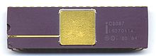
The 8087 was an advanced integrated circuit, pushing the limits of manufacturing technology of the period.[citation needed] Basic operations on the 8087 such as addition and subtraction can take over 100 machine cycles to execute and some instructions exceed 1000 cycles.[8] The chip lacks a hardware multiplier and implements calculations using the CORDIC algorithm.[9]
Sales of the 8087 received a significant boost when a coprocessor socket was included on the 1981 IBM PC motherboard. Development of the 8087 led to the IEEE 754-1985 standard for floating-point arithmetic. The available speed version were 4.77 (5), 8, and 10 MHz.[10] There were later x87 coprocessors for the 80186, 80286, 80386, and 80386SX processors. Starting with the 80486, the later Intel x86 processors did not use a separate floating-point coprocessor; floating-point functions were integrated with the processor.
Intel 80186 and its associated products were discontinued on March 30, 2007 for orders and September 28, 2007 for shipments.[11]
Intel had previously manufactured the 8231Arithmetic processing unit, and the 8232Floating Point Processor. These were designed for use with 8080 or similar processors and used an 8-bit data bus. They were interfaced to a host system either through programmed I/O or a DMA controller.[13]
The 8087 was initially conceived by Bill Pohlman, the engineering manager at Intel who oversaw the development of the 8086 chip. Bill took steps to be sure that the 8086 chip could support a yet-to-be-developed math chip.
In 1977 Pohlman got the go ahead to design the 8087 math chip. Bruce Ravenel was assigned as architect, and John Palmer was hired to be co-architect and mathematician for the project. The two came up with a revolutionary design with 64 bits of mantissa and 16 bits of exponent for the longest-format real number, with a stack architecture CPU and eight 80-bit stack registers, with a computationally rich instruction set. The design solved a few outstanding known problems in numerical computing and numerical software: rounding-error problems were eliminated for 64-bit operands, and numerical mode conversions were solved for all 64-bit numbers. Palmer credited William Kahan's writings on floating point as a significant influence on their design.[14]
The 8087 design initially met a cool reception in Santa Clara due to its aggressive design. Eventually, the design was assigned to Intel Israel, and Rafi Nave was assigned to lead the implementation of the chip. Palmer, Ravenel and Nave were awarded patents for the design.[15] Robert Koehler and John Bayliss were also awarded a patent for the technique where some instructions with a particular bit pattern were offloaded to the coprocessor.[16]
The 8087 had 65,000transistors and was manufactured as a 4.5μm (then shrunk to 3μm) depletion-load HMOS circuit. It worked in tandem with the 8086 or 8088 and introduced about 60 new instructions. Most 8087 assembly mnemonics begin with F, such as FADD, FMUL, FCOM and so on, making them easily distinguishable from 8086 instructions. The binary encodings for all 8087 instructions begin with the bit pattern 11011, decimal 27, the same as the ASCII character ESC, although in the higher-order bits of a byte; similar instruction prefixes are also sometimes referred to as "escape codes". The instruction mnemonic assigned by Intel for these coprocessor instructions is "ESC".
When the 8086 or 8088 CPU executed the ESC instruction, if the second byte (the ModR/M byte) specified a memory operand, the CPU would execute a bus cycle to read one word from the memory location specified in the instruction (using any 8086 addressing mode), but it would not store the read operand into any CPU register or perform any operation on it; the 8087 would observe the bus and decode the instruction stream in sync with the 8086, recognizing the coprocessor instructions meant for itself. For an 8087 instruction with a memory operand, if the instruction called for the operand to be read, the 8087 would take the word of data read by the main CPU from the data bus. If the operand to be read was longer than one word, the 8087 would also copy the address from the address bus; then, after completion of the data read cycle driven by the CPU, the 8087 would immediately use DMA to take control of the bus and transfer the additional bytes of the operand itself. If an 8087 instruction with a memory operand called for that operand to be written, the 8087 would ignore the read word on the data bus and just copy the address, then request DMA and write the entire operand, in the same way that it would read the end of an extended operand. In this way, the main CPU maintained general control of the bus and bus timing, while the 8087 handled all other aspects of execution of coprocessor instructions, except for brief DMA periods when the 8087 would take over the bus to read or write operands to/from its own internal registers. As a consequence of this design, the 8087 could only operate on operands taken either from memory or from its own registers, and any exchange of data between the 8087 and the 8086 or 8088 was only through RAM.
The main CPU program continued to execute while the 8087 executed an instruction; from the perspective of the main 8086 or 8088 CPU, a coprocessor instruction took only as long as the processing of the opcode and any memory operand cycle (2 clock cycles for no operand, 8 clock cycles plus the EA calculation time [5 to 12 clock cycles] for a memory operand [plus 4 more clock cycles on an 8088], to transfer the second byte of the operand word), after which the CPU would begin executing the next instruction of the program. Thus, a system with an 8087 was capable of true parallel processing, performing one operation in the integer ALU of the main CPU while at the same time performing a floating-point operation in the 8087 coprocessor. Since the 8086 or 8088 exclusively controlled the instruction flow and timing and had no direct access to the internal status of the 8087, and because the 8087 could execute only one instruction at a time, programs for the combined 8086/8087 or 8088/8087 system had to ensure that the 8087 had time to complete the last instruction issued to it before it was issued another one. The WAIT instruction (of the main CPU) was provided for this purpose, and most assemblers implicitly asserted a WAIT instruction before each instance of most floating-point coprocessor instructions. (It is not necessary to use a WAIT instruction before an 8087 operation if the program uses other means to ensure that enough time elapses between the issuance of timing-sensitive 8087 instructions so that the 8087 can never receive such an instruction before it completes the previous one. It is also not necessary, if a WAIT is used, that it immediately precede the next 8087 instruction.) The WAIT instruction waited for the −TEST input pin of the 8086/8088 to be asserted (low), and this pin was connected to the BUSY pin of the 8087 in all systems that had an 8087 (so TEST was asserted when BUSY was deasserted).
Because the instruction prefetch queues of the 8086 and 8088 make the time when an instruction is executed not always the same as the time it is fetched, a coprocessor such as the 8087 cannot determine when an instruction for itself is the next instruction to be executed purely by watching the CPU bus. The 8086 and 8088 have two queue status signals connected to the coprocessor to allow it to synchronize with the CPU's internal timing of execution of instructions from its prefetch queue. The 8087 maintains its own identical prefetch queue, from which it reads the coprocessor opcodes that it actually executes. Because the 8086 and 8088 prefetch queues have different sizes and different management algorithms, the 8087 determines which type of CPU it is attached to by observing a certain CPU bus line when the system is reset, and the 8087 adjusts its internal instruction queue accordingly. The redundant duplication of prefetch queue hardware in the CPU and the coprocessor is inefficient in terms of power usage and total die area, but it allowed the coprocessor interface to use very few dedicated IC pins, which was important. At the time when the 8086, which defined the coprocessor interface, was introduced, IC packages with more than 40 pins were rare, expensive, and wrangled with problems such as excessive lead capacitance, a major limiting factor for signalling speeds.
The coprocessor operation codes are encoded in 6 bits across 2 bytes, beginning with the escape sequence:
The first three "x" bits are the first three bits of the floating-point opcode. Then two "m" bits, then the latter half three bits of the floating-point opcode, followed by three "r" bits. The "m" and "r" bits specify the addressing-mode information.[17]
Application programs had to be written to make use of the special floating-point instructions. At run time, software could detect the coprocessor and use it for floating-point operations. When detected absent, similar floating-point functions had to be calculated in software, or the whole coprocessor could be emulated in software for more precise numerical compatibility.[18]
Registers
Simplified 8087 microarchitecture
The x87 family does not use a directly addressable register set such as the main registers of the x86 processors; instead, the x87 registers form an eight-level deep stack structure[19] ranging from st0 to st7, where st0 is the top. The x87 instructions operate by pushing, calculating, and popping values on this stack. However, dyadic operations such as FADD, FMUL, FCMP, and so on may either implicitly use the topmost st0 and st1 or may use st0 together with an explicit memory operand or register; the st0 register may thus be used as an accumulator (i.e. as a combined destination and left operand) and can also be exchanged with any of the eight stack registers using an instruction called FXCH stX (codes D9C8–D9CFh). This makes the x87 stack usable as seven freely addressable registers plus an accumulator. This is especially applicable on superscalar x86 processors (Pentium of 1993 and later), where these exchange instructions are optimized down to a zero-clock penalty.
IEEE floating-point standard
When Intel designed the 8087, it aimed to make a standard floating-point format for future designs. An important aspect of the 8087 from a historical perspective was that it became the basis for the IEEE 754 floating-point standard. The 8087 did not implement the eventual IEEE 754 standard in all its details, as the standard was not finished until 1985, but the 80387 did. The 8087 provided two basic 32/64-bit floating-point data types and an additional extended 80-bit internal temporary format (that could also be stored in memory) to improve accuracy over large and complex calculations. Apart from this, the 8087 offered an 80-bit/18-digit packed BCD (binary-coded decimal) format and 16-, 32-, and 64-bit integer data types.[19]
8087 data types
79
...
71
...
67
...
63
...
50
...
31
...
22
...
15
...
00
(bit position)
±
Exponent
Fraction
80-bit extended-precision real
±
Exponent
Fraction
64-bit double-precision real
±
Exponent
Fraction
32-bit single-precision real
±
BCD Integer
18-digit decimal integer
±
Integer
64-bit binary integer
±
Integer
32-bit binary integer
±
Integer
16-bit binary integer
Infinity
The 8087 handles infinity values by either affine closure or projective closure (selected by the status register). With affine closure, positive and negative infinities are treated as different values. With projective closure, infinity is treated as an unsigned representation for very small or very large numbers.[20] These two methods of handling infinity were incorporated into the draft version of the IEEE 754 floating-point standard. However, projective closure (projectively extended real number system) was dropped from the later formal issue of IEEE 754-1985. The 80287 retained projective closure as an option, but the 80387 and subsequent floating-point processors (including the 80187) only supported affine closure.
Coprocessor interface
The 8087 differed from subsequent Intel coprocessors in that it was directly connected to the address and data buses. The 8087 looked for instructions that commenced with the "11011" sequence and acted on them, immediately requesting DMA from the main CPU as necessary to access memory operands longer than one word (16bits), then immediately releasing bus control back to the main CPU. The coprocessor did not hold up execution of the program until the coprocessor instruction was complete, and the program had to explicitly synchronize the two processors, as explained above (in the "Design and development" section). There was a potential crash problem if the coprocessor instruction failed to decode to one that the coprocessor understood. Intel's later coprocessors did not connect to the buses in the same way, but received instructions through the main processor I/O ports. This yielded an execution time penalty, but the potential crash problem was avoided because the main processor would ignore the instruction if the coprocessor refused to accept it. The 8087 was able to detect whether it was connected to an 8088 or an 8086 by monitoring the data bus during the reset cycle.
The 8087 was, in theory, capable of working concurrently while the 8086/8 processes additional instructions. In practice, there was the potential for program failure if the coprocessor issued a new instruction before the last one had completed. The assembler would automatically insert an FWAIT instruction after every coprocessor opcode, forcing the 8086/8 to halt execution until the 8087 signalled that it had finished.[21] This limitation was removed from later designs.
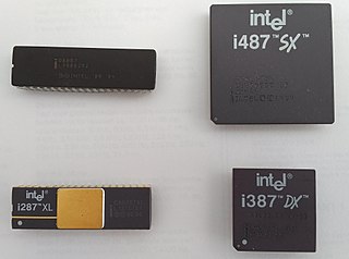
Successors
Just as the 8088 and 8086 processors were superseded by later parts, so was the 8087 superseded. Other Intel coprocessors were the 80287 (actually - 80C287, as Intel moved to a CMOS process by that time), 80387, and the 80187. Starting with the 80486, the later Intel processors did not use a separate floating-point coprocessor; virtually all included it on the main processor die, with the significant exception of the 80486SX, which was a modified 80486DX with the FPU disabled. 80487 was in fact a full-blown 80486DX chip with an extra pin. When installed, it disabled the 80486SX CPU. The 80486DX, Pentium, and later processors include floating-point functionality on the CPU core.
Related Research Articles
The Intel 80286 is a 16-bit microprocessor that was introduced on February 1, 1982. It was the first 8086-based CPU with separate, non-multiplexed address and data buses and also the first with memory management and wide protection abilities. The 80286 used approximately 134,000 transistors in its original nMOS (HMOS) incarnation and, just like the contemporary 80186, it could correctly execute most software written for the earlier Intel 8086 and 8088 processors.
The Intel 8080 ("eighty-eighty") is the second 8-bit microprocessor designed and manufactured by Intel. It first appeared in April 1974 and is an extended and enhanced variant of the earlier 8008 design, although without binary compatibility. The initial specified clock rate or frequency limit was 2 MHz, with common instructions using 4, 5, 7, 10, or 11 cycles. As a result, the processor is able to execute several hundred thousand instructions per second. Two faster variants, the 8080A-1 and 8080A-2, became available later with clock frequency limits of 3.125 MHz and 2.63 MHz respectively. The 8080 needs two support chips to function in most applications: the i8224 clock generator/driver and the i8228 bus controller. It is implemented in N-type metal–oxide–semiconductor logic (NMOS) using non-saturated enhancement mode transistors as loads thus demanding a +12 V and a −5 V voltage in addition to the main transistor–transistor logic (TTL) compatible +5 V.
The 8086 is a 16-bit microprocessor chip designed by Intel between early 1976 and June 8, 1978, when it was released. The Intel 8088, released July 1, 1979, is a slightly modified chip with an external 8-bit data bus, and is notable as the processor used in the original IBM PC design.
The Intel 8088 microprocessor is a variant of the Intel 8086. Introduced on June 1, 1979, the 8088 has an eight-bit external data bus instead of the 16-bit bus of the 8086. The 16-bit registers and the one megabyte address range are unchanged, however. In fact, according to the Intel documentation, the 8086 and 8088 have the same execution unit (EU)—only the bus interface unit (BIU) is different. The 8088 was used in the original IBM PC and in IBM PC compatible clones.
x86 is a family of complex instruction set computer (CISC) instruction set architectures initially developed by Intel based on the Intel 8086 microprocessor and its 8088 variant. The 8086 was introduced in 1978 as a fully 16-bit extension of Intel's 8-bit 8080 microprocessor, with memory segmentation as a solution for addressing more memory than can be covered by a plain 16-bit address. The term "x86" came into being because the names of several successors to Intel's 8086 processor end in "86", including the 80186, 80286, 80386 and 80486 processors. Colloquially, their names were "186", "286", "386" and "486".
The Z80 is an 8-bit microprocessor introduced by Zilog as the startup company's first product. The Z80 was conceived by Federico Faggin in late 1974 and developed by him and his 11 employees starting in early 1975. The first working samples were delivered in March 1976, and it was officially introduced on the market in July 1976. With the revenue from the Z80, the company built its own chip factories and grew to over a thousand employees over the following two years.
A floating-point unit is a part of a computer system specially designed to carry out operations on floating-point numbers. Typical operations are addition, subtraction, multiplication, division, and square root. Some FPUs can also perform various transcendental functions such as exponential or trigonometric calculations, but the accuracy can be low, so some systems prefer to compute these functions in software.
MMX is a single instruction, multiple data (SIMD) instruction set architecture designed by Intel, introduced on January 8, 1997 with its Pentium P5 (microarchitecture) based line of microprocessors, named "Pentium with MMX Technology". It developed out of a similar unit introduced on the Intel i860, and earlier the Intel i750 video pixel processor. MMX is a processor supplementary capability that is supported on IA-32 processors by Intel and other vendors as of 1997. AMD also added MMX instruction set in its K6 processor.
The Intel 8085 ("eighty-eighty-five") is an 8-bit microprocessor produced by Intel and introduced in March 1976. It is the last 8-bit microprocessor developed by Intel.
x86 assembly language is the name for the family of assembly languages which provide some level of backward compatibility with CPUs back to the Intel 8008 microprocessor, which was launched in April 1972. It is used to produce object code for the x86 class of processors.
A coprocessor is a computer processor used to supplement the functions of the primary processor. Operations performed by the coprocessor may be floating-point arithmetic, graphics, signal processing, string processing, cryptography or I/O interfacing with peripheral devices. By offloading processor-intensive tasks from the main processor, coprocessors can accelerate system performance. Coprocessors allow a line of computers to be customized, so that customers who do not need the extra performance do not need to pay for it.
Fetching the instruction opcodes from program memory well in advance is known as prefetching and it is served by using a prefetch input queue (PIQ). The pre-fetched instructions are stored in a queue. The fetching of opcodes well in advance, prior to their need for execution, increases the overall efficiency of the processor boosting its speed. The processor no longer has to wait for the memory access operations for the subsequent instruction opcode to complete. This architecture was prominently used in the Intel 8086 microprocessor.
The NEC V20 is a microprocessor that was designed and produced by NEC. It is both pin compatible and object code compatible with the Intel 8088, with an instruction set architecture (ISA) similar to that of the Intel 80188 with some extensions. The V20 was introduced in March 1984.
The x86 instruction set refers to the set of instructions that x86-compatible microprocessors support. The instructions are usually part of an executable program, often stored as a computer file and executed on the processor.
The TMS9900 was one of the first commercially available, single-chip 16-bit microprocessors. Introduced in June 1976, it implemented Texas Instruments' TI-990 minicomputer architecture in a single-chip format, and was initially used for low-end models of that lineup.
x87 is a floating-point-related subset of the x86 architecture instruction set. It originated as an extension of the 8086 instruction set in the form of optional floating-point coprocessors that work in tandem with corresponding x86 CPUs. These microchips have names ending in "87". This is also known as the NPX. Like other extensions to the basic instruction set, x87 instructions are not strictly needed to construct working programs, but provide hardware and microcode implementations of common numerical tasks, allowing these tasks to be performed much faster than corresponding machine code routines can. The x87 instruction set includes instructions for basic floating-point operations such as addition, subtraction and comparison, but also for more complex numerical operations, such as the computation of the tangent function and its inverse, for example.
Each time Intel launched a new microprocessor, they simultaneously provided a system development kit (SDK) allowing engineers, university students, and others to familiarise themselves with the new processor's concepts and features. The SDK single-board computers allowed the user to enter object code from a keyboard or upload it through a communication port, and then test run the code. The SDK boards provided a system monitor ROM to operate the keyboard and other interfaces. Kits varied in their specific features but generally offered optional memory and interface configurations, a serial terminal link, audio cassette storage, and EPROM program memory. Intel's Intellec development system could download code to the SDK boards.
The Intel 8089 input/output coprocessor was available for use with the 8086/8088 central processor. It was announced in May 1979, but the price was not available at that time. It used the same programming technique as 8087 for input/output operations, such as transfer of data from memory to a peripheral device, and so reducing the load on the CPU. This I/O processor was available in July 1979 for US$194.20 in quantities of 100 or more. Intel second sourced this coprocessor to Fujitsu Limited.
The Intel 8231 and 8232 were early designs of floating-point maths coprocessors (FPUs), marketed for use with their i8080 line of primary CPUs. They were licensed versions of AMD's Am9511 and Am9512 FPUs, from 1977 and 1979, themselves claimed by AMD as the world's first single-chip FPU solutions.
↑ Shirriff, Ken (May 2020). "Extracting ROM constants from the 8087 math coprocessor's die". righto.com. Self-published by Ken Shirriff. Retrieved 3 September 2020. The ROM contains 16 arctangent values, the arctans of 2−n. It also contains 14 log values, the base-2 logs of (1+2−n). These may seem like unusual values, but they are used in an efficient algorithm called CORDIC, which was invented in 1958.
↑ Yoshida, Stacy, "Math Coprocessors: Keeping Your Computer Up for the Count", Intel Corporation, Microcomputer Solutions, September/October 1990, page 16
This page is based on this Wikipedia article Text is available under the CC BY-SA 4.0 license; additional terms may apply. Images, videos and audio are available under their respective licenses.