
A central processing unit (CPU)—also called a central processor or main processor—is the most important processor in a given computer. Its electronic circuitry executes instructions of a computer program, such as arithmetic, logic, controlling, and input/output (I/O) operations. This role contrasts with that of external components, such as main memory and I/O circuitry, and specialized coprocessors such as graphics processing units (GPUs).
In processor design, microcode serves as an intermediary layer situated between the central processing unit (CPU) hardware and the programmer-visible instruction set architecture of a computer, also known as its machine code. It consists of a set of hardware-level instructions that implement the higher-level machine code instructions or control internal finite-state machine sequencing in many digital processing components. While microcode is utilized in general-purpose CPUs in contemporary desktops, it also functions as a fallback path for scenarios that the faster hardwired control unit is unable to manage.

The Pentium is a x86 microprocessor introduced by Intel on March 22, 1993. It is the first CPU using the Pentium brand. Considered the fifth generation in the 8086 compatible line of processors, its implementation and microarchitecture was internally called P5.

The Pentium Pro is a sixth-generation x86 microprocessor developed and manufactured by Intel and introduced on November 1, 1995. It introduced the P6 microarchitecture and was originally intended to replace the original Pentium in a full range of applications. While the Pentium and Pentium MMX had 3.1 and 4.5 million transistors, respectively, the Pentium Pro contained 5.5 million transistors. Later, it was reduced to a more narrow role as a server and high-end desktop processor and was used in supercomputers like ASCI Red, the first computer to reach the trillion floating point operations per second (teraFLOPS) performance mark in 1996. The Pentium Pro was capable of both dual- and quad-processor configurations. It only came in one form factor, the relatively large rectangular Socket 8. The Pentium Pro was succeeded by the Pentium II Xeon in 1998.
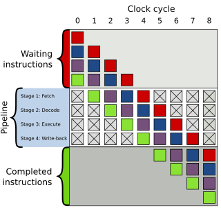
In computer engineering, instruction pipelining is a technique for implementing instruction-level parallelism within a single processor. Pipelining attempts to keep every part of the processor busy with some instruction by dividing incoming instructions into a series of sequential steps performed by different processor units with different parts of instructions processed in parallel.
In the history of computer hardware, some early reduced instruction set computer central processing units used a very similar architectural solution, now called a classic RISC pipeline. Those CPUs were: MIPS, SPARC, Motorola 88000, and later the notional CPU DLX invented for education.
In computer architecture, a branch predictor is a digital circuit that tries to guess which way a branch will go before this is known definitively. The purpose of the branch predictor is to improve the flow in the instruction pipeline. Branch predictors play a critical role in achieving high performance in many modern pipelined microprocessor architectures.
The NetBurst microarchitecture, called P68 inside Intel, was the successor to the P6 microarchitecture in the x86 family of central processing units (CPUs) made by Intel. The first CPU to use this architecture was the Willamette-core Pentium 4, released on November 20, 2000 and the first of the Pentium 4 CPUs; all subsequent Pentium 4 and Pentium D variants have also been based on NetBurst. In mid-2001, Intel released the Foster core, which was also based on NetBurst, thus switching the Xeon CPUs to the new architecture as well. Pentium 4-based Celeron CPUs also use the NetBurst architecture.
A CPU cache is a hardware cache used by the central processing unit (CPU) of a computer to reduce the average cost to access data from the main memory. A cache is a smaller, faster memory, located closer to a processor core, which stores copies of the data from frequently used main memory locations. Most CPUs have a hierarchy of multiple cache levels, with different instruction-specific and data-specific caches at level 1. The cache memory is typically implemented with static random-access memory (SRAM), in modern CPUs by far the largest part of them by chip area, but SRAM is not always used for all levels, or even any level, sometimes some latter or all levels are implemented with eDRAM.

In electronics, computer science and computer engineering, microarchitecture, also called computer organization and sometimes abbreviated as µarch or uarch, is the way a given instruction set architecture (ISA) is implemented in a particular processor. A given ISA may be implemented with different microarchitectures; implementations may vary due to different goals of a given design or due to shifts in technology.
In computer architecture, a branch target predictor is the part of a processor that predicts the target, i.e. the address of the instruction that is executed next, of a taken conditional branch or an unconditional branch instruction before the target of the branch instruction is computed by the execution unit of the processor.
The P6 microarchitecture is the sixth-generation Intel x86 microarchitecture, implemented by the Pentium Pro microprocessor that was introduced in November 1995. It is frequently referred to as i686. It was planned to be succeeded by the NetBurst microarchitecture used by the Pentium 4 in 2000, but was revived for the Pentium M line of microprocessors. The successor to the Pentium M variant of the P6 microarchitecture is the Core microarchitecture which in turn is also derived from P6.
The Intel Core microarchitecture is a multi-core processor microarchitecture launched by Intel in mid-2006. It is a major evolution over the Yonah, the previous iteration of the P6 microarchitecture series which started in 1995 with Pentium Pro. It also replaced the NetBurst microarchitecture, which suffered from high power consumption and heat intensity due to an inefficient pipeline designed for high clock rate. In early 2004 the new version of NetBurst (Prescott) needed very high power to reach the clocks it needed for competitive performance, making it unsuitable for the shift to dual/multi-core CPUs. On May 7, 2004 Intel confirmed the cancellation of the next NetBurst, Tejas and Jayhawk. Intel had been developing Merom, the 64-bit evolution of the Pentium M, since 2001, and decided to expand it to all market segments, replacing NetBurst in desktop computers and servers. It inherited from Pentium M the choice of a short and efficient pipeline, delivering superior performance despite not reaching the high clocks of NetBurst.

In computer central processing units, micro-operations are detailed low-level instructions used in some designs to implement complex machine instructions.
Goldmont is a microarchitecture for low-power Atom, Celeron and Pentium branded processors used in systems on a chip (SoCs) made by Intel. They allow only one thread per core.
Goldmont Plus is a microarchitecture for low-power Atom, Celeron and Pentium Silver branded processors used in systems on a chip (SoCs) made by Intel. The Gemini Lake platform with 14 nm Goldmont Plus core was officially launched on December 11, 2017. Intel launched the Gemini Lake Refresh platform on November 4, 2019.
Intel microcode is microcode that runs inside x86 processors made by Intel. Since the P6 microarchitecture introduced in the mid-1990s, the microcode programs can be patched by the operating system or BIOS firmware to work around bugs found in the CPU after release. Intel had originally designed microcode updates for processor debugging under its design for testing (DFT) initiative.
Tremont is a microarchitecture for low-power Atom, Celeron and Pentium Silver branded processors used in systems on a chip (SoCs) made by Intel. It is the successor to Goldmont Plus. Intel officially launched Elkhart Lake platform with 10 nm Tremont core on September 23, 2020. Intel officially launched Jasper Lake platform with 10 nm Tremont core on January 11, 2021.
Golden Cove is a codename for a CPU microarchitecture developed by Intel and released in November 2021. It succeeds four microarchitectures: Sunny Cove, Skylake, Willow Cove, and Cypress Cove. It is fabricated using Intel's Intel 7 process node, previously referred to as 10 nm Enhanced SuperFin (10ESF).

