Harvard architecture

Last updated

Harvard architecture Harvard architecture.svg
Harvard architecture

The Harvard architecture is a computer architecture with separate storage and signal pathways for instructions and data. It is often contrasted with the von Neumann architecture, where program instructions and data share the same memory and pathways.

Contents

The term is often stated as having originated from the Harvard Mark I relay-based computer, which stored instructions on punched tape (24 bits wide) and data in electro-mechanical counters. These early machines had data storage entirely contained within the central processing unit, and provided no access to the instruction storage as data. Programs needed to be loaded by an operator; the processor could not initialize itself. However, in the only peer-reviewed published paper on the topic The Myth of the Harvard Architecture published in the IEEE Annals of the History of Computing [1]  the author demonstrates that:

Modern processors appear to the user to be systems with von Neumann architectures, with the program code stored in the same main memory as the data. For performance reasons, internally and largely invisible to the user, most designs have separate processor caches for the instructions and data, with separate pathways into the processor for each. This is one form of what is known as the modified Harvard architecture.

Harvard architecture is historically, and traditionally, split into two address spaces, but having three, i.e. two extra (and all accessed in each cycle) is also done, [2] while rare.

Memory details

In a Harvard architecture, there is no need to make the two memories share characteristics. In particular, the word width, timing, implementation technology, and memory address structure can differ. In some systems, instructions for pre-programmed tasks can be stored in read-only memory while data memory generally requires read-write memory. In some systems, there is much more instruction memory than data memory so instruction addresses are wider than data addresses.

Contrast with von Neumann architectures

In a system with a pure von Neumann architecture, instructions and data are stored in the same memory, so instructions are fetched over the same data path used to fetch data. This means that a CPU cannot simultaneously read an instruction and read or write data from or to the memory. In a computer using the Harvard architecture, the CPU can both read an instruction and perform a data memory access at the same time, [3] even without a cache. A Harvard architecture computer can thus be faster for a given circuit complexity because instruction fetches and data access do not contend for a single memory pathway.

Also, a Harvard architecture machine has distinct code and data address spaces: instruction address zero is not the same as data address zero. Instruction address zero might identify a twenty-four-bit value, while data address zero might indicate an eight-bit byte that is not part of that twenty-four-bit value.

Contrast with modified Harvard architecture

A modified Harvard architecture machine is very much like a Harvard architecture machine, but it relaxes the strict separation between instruction and data while still letting the CPU concurrently access two (or more) memory buses. The most common modification includes separate instruction and data caches backed by a common address space. While the CPU executes from cache, it acts as a pure Harvard machine. When accessing backing memory, it acts like a von Neumann machine (where code can be moved around like data, which is a powerful technique). This modification is widespread in modern processors, such as the ARM architecture, Power ISA and x86 processors. It is sometimes loosely called a Harvard architecture, overlooking the fact that it is actually "modified".

Another modification provides a pathway between the instruction memory (such as ROM or flash memory) and the CPU to allow words from the instruction memory to be treated as read-only data. This technique is used in some microcontrollers, including the Atmel AVR. This allows constant data, such as text strings or function tables, to be accessed without first having to be copied into data memory, preserving scarce (and power-hungry) data memory for read/write variables. Special machine language instructions are provided to read data from the instruction memory, or the instruction memory can be accessed using a peripheral interface. [lower-alpha 1] (This is distinct from instructions which themselves embed constant data, although for individual constants the two mechanisms can substitute for each other.)

Speed

In recent years, the speed of the CPU has grown many times in comparison to the access speed of the main memory. Care needs to be taken to reduce the number of times main memory is accessed in order to maintain performance. If, for instance, every instruction run in the CPU requires an access to memory, the computer gains nothing for increased CPU speed—a problem referred to as being memory bound.

It is possible to make extremely fast memory, but this is only practical for small amounts of memory for cost, power and signal routing reasons. The solution is to provide a small amount of very fast memory known as a CPU cache which holds recently accessed data. As long as the data that the CPU needs is in the cache, the performance is much higher than it is when the CPU has to get the data from the main memory. On the other side, however, it may still be limited to storing repetitive programs or data and still has a storage size limitation, and other potential problems associated with it. [lower-alpha 2]

Internal vs. external design

Modern high performance CPU chip designs incorporate aspects of both Harvard and von Neumann architecture. In particular, the "split cache" version of the modified Harvard architecture is very common. CPU cache memory is divided into an instruction cache and a data cache. Harvard architecture is used as the CPU accesses the cache. In the case of a cache miss, however, the data is retrieved from the main memory, which is not formally divided into separate instruction and data sections, although it may well have separate memory controllers used for concurrent access to RAM, ROM and (NOR) flash memory.

Thus, while a von Neumann architecture is visible in some contexts, such as when data and code come through the same memory controller, the hardware implementation gains the efficiencies of the Harvard architecture for cache accesses and at least some main memory accesses.

In addition, CPUs often have write buffers which let CPUs proceed after writes to non-cached regions. The von Neumann nature of memory is then visible when instructions are written as data by the CPU and software must ensure that the caches (data and instruction) and write buffer are synchronized before trying to execute those just-written instructions.

Modern uses of the Harvard architecture

The principal advantage of the pure Harvard architecture—simultaneous access to more than one memory system—has been reduced by modified Harvard processors using modern CPU cache systems. Relatively pure Harvard architecture machines are used mostly in applications where trade-offs, like the cost and power savings from omitting caches, outweigh the programming penalties from featuring distinct code and data address spaces.

Even in these cases, it is common to employ special instructions in order to access program memory as though it were data for read-only tables, or for reprogramming; those processors are modified Harvard architecture processors.

Notes

  1. The IAP lines of 8051-compatible microcontrollers from STC have dual ported Flash memory, with one of the two ports hooked to the instruction bus of the processor core, and the other port made available in the special function register region.
  2. As in a well described case of Intel 80486. [4] :26–34 [5]

Related Research Articles

<span class="mw-page-title-main">Central processing unit</span> Central computer component which executes instructions

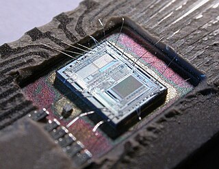
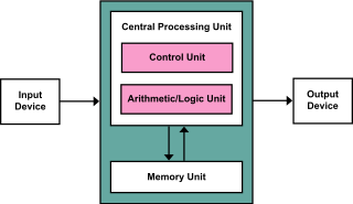
A central processing unit (CPU)—also called a central processor or main processor—is the most important processor in a given computer. Its electronic circuitry executes instructions of a computer program, such as arithmetic, logic, controlling, and input/output (I/O) operations. This role contrasts with that of external components, such as main memory and I/O circuitry, and specialized coprocessors such as graphics processing units (GPUs).

<span class="mw-page-title-main">Microcontroller</span> Small computer on a single integrated circuit

A microcontroller or microcontroller unit (MCU) is a small computer on a single integrated circuit. A microcontroller contains one or more CPUs along with memory and programmable input/output peripherals. Program memory in the form of ferroelectric RAM, NOR flash or OTP ROM is also often included on chip, as well as a small amount of RAM. Microcontrollers are designed for embedded applications, in contrast to the microprocessors used in personal computers or other general purpose applications consisting of various discrete chips.

<span class="mw-page-title-main">Program counter</span> Processor register that indicates where a computer is in its program sequence

The program counter (PC), commonly called the instruction pointer (IP) in Intel x86 and Itanium microprocessors, and sometimes called the instruction address register (IAR), the instruction counter, or just part of the instruction sequencer, is a processor register that indicates where a computer is in its program sequence.

<span class="mw-page-title-main">MCS-51</span> Single chip microcontroller series by Intel

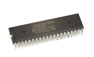
The Intel MCS-51 is a single chip microcontroller (MCU) series developed by Intel in 1980 for use in embedded systems. The architect of the Intel MCS-51 instruction set was John H. Wharton. Intel's original versions were popular in the 1980s and early 1990s, and enhanced binary compatible derivatives remain popular today. It is a complex instruction set computer, but also has some of the features of RISC architectures, such as a large register set and register windows, and has separate memory spaces for program instructions and data.

SuperH is a 32-bit reduced instruction set computing (RISC) instruction set architecture (ISA) developed by Hitachi and currently produced by Renesas. It is implemented by microcontrollers and microprocessors for embedded systems.

<span class="mw-page-title-main">Digital signal processor</span> Specialized microprocessor optimized for digital signal processing

A digital signal processor (DSP) is a specialized microprocessor chip, with its architecture optimized for the operational needs of digital signal processing. DSPs are fabricated on metal–oxide–semiconductor (MOS) integrated circuit chips. They are widely used in audio signal processing, telecommunications, digital image processing, radar, sonar and speech recognition systems, and in common consumer electronic devices such as mobile phones, disk drives and high-definition television (HDTV) products.

<span class="mw-page-title-main">PIC microcontrollers</span> Line of single-chip microprocessors from Microchip Technology

PIC is a family of microcontrollers made by Microchip Technology, derived from the PIC1650 originally developed by General Instrument's Microelectronics Division. The name PIC initially referred to Peripheral Interface Controller, and is currently expanded as Programmable Intelligent Computer. The first parts of the family were available in 1976; by 2013 the company had shipped more than twelve billion individual parts, used in a wide variety of embedded systems.

In computer science, self-modifying code is code that alters its own instructions while it is executing – usually to reduce the instruction path length and improve performance or simply to reduce otherwise repetitively similar code, thus simplifying maintenance. The term is usually only applied to code where the self-modification is intentional, not in situations where code accidentally modifies itself due to an error such as a buffer overflow.

Memory-mapped I/O (MMIO) and port-mapped I/O (PMIO) are two complementary methods of performing input/output (I/O) between the central processing unit (CPU) and peripheral devices in a computer. An alternative approach is using dedicated I/O processors, commonly known as channels on mainframe computers, which execute their own instructions.

von Neumann architecture Computer architecture where code and data share a common bus

The von Neumann architecture—also known as the von Neumann model or Princeton architecture—is a computer architecture based on a 1945 description by John von Neumann, and by others, in the First Draft of a Report on the EDVAC. The document describes a design architecture for an electronic digital computer with these components:

A processor register is a quickly accessible location available to a computer's processor. Registers usually consist of a small amount of fast storage, although some registers have specific hardware functions, and may be read-only or write-only. In computer architecture, registers are typically addressed by mechanisms other than main memory, but may in some cases be assigned a memory address e.g. DEC PDP-10, ICT 1900.

A translation lookaside buffer (TLB) is a memory cache that stores the recent translations of virtual memory to physical memory. It is used to reduce the time taken to access a user memory location. It can be called an address-translation cache. It is a part of the chip's memory-management unit (MMU). A TLB may reside between the CPU and the CPU cache, between CPU cache and the main memory or between the different levels of the multi-level cache. The majority of desktop, laptop, and server processors include one or more TLBs in the memory-management hardware, and it is nearly always present in any processor that utilizes paged or segmented virtual memory.

<span class="mw-page-title-main">Memory address</span> Reference to a specific memory location

In computing, a memory address is a reference to a specific memory location used at various levels by software and hardware. Memory addresses are fixed-length sequences of digits conventionally displayed and manipulated as unsigned integers. Such numerical semantic bases itself upon features of CPU, as well upon use of the memory like an array endorsed by various programming languages.

A CPU cache is a hardware cache used by the central processing unit (CPU) of a computer to reduce the average cost to access data from the main memory. A cache is a smaller, faster memory, located closer to a processor core, which stores copies of the data from frequently used main memory locations. Most CPUs have a hierarchy of multiple cache levels, with different instruction-specific and data-specific caches at level 1. The cache memory is typically implemented with static random-access memory (SRAM), in modern CPUs by far the largest part of them by chip area, but SRAM is not always used for all levels, or even any level, sometimes some latter or all levels are implemented with eDRAM.

<span class="mw-page-title-main">Blackfin</span> Family of 16-/32-bit microprocessors

The Blackfin is a family of 16-/32-bit microprocessors developed, manufactured and marketed by Analog Devices. The processors have built-in, fixed-point digital signal processor (DSP) functionality supplied by 16-bit multiply–accumulates (MACs), accompanied on-chip by a microcontroller. It was designed for a unified low-power processor architecture that can run operating systems while simultaneously handling complex numeric tasks such as real-time H.264 video encoding.

<span class="mw-page-title-main">Hardware acceleration</span> Specialized computer hardware

Hardware acceleration is the use of computer hardware designed to perform specific functions more efficiently when compared to software running on a general-purpose central processing unit (CPU). Any transformation of data that can be calculated in software running on a generic CPU can also be calculated in custom-made hardware, or in some mix of both.

ARM9 is a group of 32-bit RISC ARM processor cores licensed by ARM Holdings for microcontroller use. The ARM9 core family consists of ARM9TDMI, ARM940T, ARM9E-S, ARM966E-S, ARM920T, ARM922T, ARM946E-S, ARM9EJ-S, ARM926EJ-S, ARM968E-S, ARM996HS. Since ARM9 cores were released from 1998 to 2006, they are no longer recommended for new IC designs, instead ARM Cortex-A, ARM Cortex-M, ARM Cortex-R cores are preferred.

A modified Harvard architecture is a variation of the Harvard computer architecture that, unlike the pure Harvard architecture, allows memory that contains instructions to be accessed as data. Most modern computers that are documented as Harvard architecture are, in fact, modified Harvard architecture.

Memory architecture describes the methods used to implement electronic computer data storage in a manner that is a combination of the fastest, most reliable, most durable, and least expensive way to store and retrieve information. Depending on the specific application, a compromise of one of these requirements may be necessary in order to improve another requirement. Memory architecture also explains how binary digits are converted into electric signals and then stored in the memory cells. And also the structure of a memory cell.

This glossary of computer hardware terms is a list of definitions of terms and concepts related to computer hardware, i.e. the physical and structural components of computers, architectural issues, and peripheral devices.

References

  1. Pawson, Richard (30 September 2022). "The Myth of the Harvard Architecture". IEEE Annals of the History of Computing. 44 (3): 59–69. doi:10.1109/MAHC.2022.3175612. S2CID   252018052.
  2. "Kalimba DSP: User guide" (PDF). July 2006. p. 18. Retrieved 2022-09-23. this is a three-bank Harvard architecture.
  3. "386 vs. 030: the Crowded Fast Lane". Dr. Dobb's Journal, January 1988.
  4. Brown, John Forrest (1994). Embedded systems programming in C and Assembly. New York: Van Nostrand Reinhold. ISBN   0-442-01817-7. OCLC   28966593.
  5. "Embedded Systems Programming: Perils of the PC Cache". users.ece.cmu.edu. Archived from the original on January 15, 2020. Retrieved 2022-05-26.