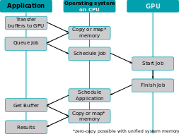
Heterogeneous System Architecture

Last updated

Heterogeneous System Architecture (HSA) is a cross-vendor set of specifications that allow for the integration of central processing units and graphics processors on the same bus, with shared memory and tasks. [1] The HSA is being developed by the HSA Foundation, which includes (among many others) AMD and ARM. The platform's stated aim is to reduce communication latency between CPUs, GPUs and other compute devices, and make these various devices more compatible from a programmer's perspective, [2] :3 [3] relieving the programmer of the task of planning the moving of data between devices' disjoint memories (as must currently be done with OpenCL or CUDA). [4]

Contents

CUDA and OpenCL as well as most other fairly advanced programming languages can use HSA to increase their execution performance. [5] Heterogeneous computing is widely used in system-on-chip devices such as tablets, smartphones, other mobile devices, and video game consoles. [6] HSA allows programs to use the graphics processor for floating point calculations without separate memory or scheduling. [7]

Rationale

The rationale behind HSA is to ease the burden on programmers when offloading calculations to the GPU. Originally driven solely by AMD and called the FSA, the idea was extended to encompass processing units other than GPUs, such as other manufacturers' DSPs, as well.

Modern GPUs are very well suited to perform single instruction, multiple data (SIMD) and single instruction, multiple threads (SIMT), while modern CPUs are still being optimized for branching. etc.

Overview

Originally introduced by embedded systems such as the Cell Broadband Engine, sharing system memory directly between multiple system actors makes heterogeneous computing more mainstream. Heterogeneous computing itself refers to systems that contain multiple processing units  central processing units (CPUs), graphics processing units (GPUs), digital signal processors (DSPs), or any type of application-specific integrated circuits (ASICs). The system architecture allows any accelerator, for instance a graphics processor, to operate at the same processing level as the system's CPU.

Among its main features, HSA defines a unified virtual address space for compute devices: where GPUs traditionally have their own memory, separate from the main (CPU) memory, HSA requires these devices to share page tables so that devices can exchange data by sharing pointers. This is to be supported by custom memory management units. [2] :6–7 To render interoperability possible and also to ease various aspects of programming, HSA is intended to be ISA-agnostic for both CPUs and accelerators, and to support high-level programming languages.

So far, the HSA specifications cover:

HSA Intermediate Layer

HSAIL (Heterogeneous System Architecture Intermediate Language), a virtual instruction set for parallel programs

HSA memory model

HSA dispatcher and run-time

Mobile devices are one of the HSA's application areas, in which it yields improved power efficiency. [6]

Block diagrams

The illustrations below compare CPU-GPU coordination under HSA versus under traditional architectures.
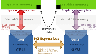
Software support

AMD GPUs contain certain additional functional units intended to be used as part of HSA. In Linux, kernel driver
.mw-parser-output .monospaced{font-family:monospace,monospace}
amdkfd provides required support. Linux AMD graphics stack.svg
AMD GPUs contain certain additional functional units intended to be used as part of HSA. In Linux, kernel driver amdkfd provides required support.

Some of the HSA-specific features implemented in the hardware need to be supported by the operating system kernel and specific device drivers. For example, support for AMD Radeon and AMD FirePro graphics cards, and APUs based on Graphics Core Next (GCN), was merged into version 3.19 of the Linux kernel mainline, released on 8 February 2015. [10] Programs do not interact directly with amdkfd[ further explanation needed ], but queue their jobs utilizing the HSA runtime. [11] This very first implementation, known as amdkfd, focuses on "Kaveri" or "Berlin" APUs and works alongside the existing Radeon kernel graphics driver.

Additionally, amdkfd supports heterogeneous queuing (HQ), which aims to simplify the distribution of computational jobs among multiple CPUs and GPUs from the programmer's perspective. Support for heterogeneous memory management (HMM), suited only for graphics hardware featuring version 2 of the AMD's IOMMU, was accepted into the Linux kernel mainline version 4.14. [12]

Integrated support for HSA platforms has been announced for the "Sumatra" release of OpenJDK, due in 2015. [13]

AMD APP SDK is AMD's proprietary software development kit targeting parallel computing, available for Microsoft Windows and Linux. Bolt is a C++ template library optimized for heterogeneous computing. [14]

GPUOpen comprehends a couple of other software tools related to HSA. CodeXL version 2.0 includes an HSA profiler. [15]

Hardware support

AMD

As of February 2015, only AMD's "Kaveri" A-series APUs (cf. "Kaveri" desktop processors and "Kaveri" mobile processors) and Sony's PlayStation 4 allowed the integrated GPU to access memory via version 2 of the AMD's IOMMU. Earlier APUs (Trinity and Richland) included the version 2 IOMMU functionality, but only for use by an external GPU connected via PCI Express.[ citation needed ]

Post-2015 Carrizo and Bristol Ridge APUs also include the version 2 IOMMU functionality for the integrated GPU.[ citation needed ]

The following table shows features of AMD's processors with 3D graphics, including APUs (see also: List of AMD processors with 3D graphics).

PlatformHigh, standard and low powerLow and ultra-low power
CodenameServerBasic Toronto
Micro Kyoto
DesktopPerformance Raphael
Mainstream Llano Trinity Richland Kaveri Kaveri Refresh (Godavari) Carrizo Bristol Ridge Raven Ridge Picasso Renoir Cezanne
Entry
Basic Kabini Dalí
MobilePerformance Renoir Cezanne Rembrandt Dragon Range
Mainstream Llano Trinity Richland Kaveri Carrizo Bristol Ridge Raven Ridge Picasso Renoir
Lucienne
Cezanne
Barceló
Phoenix
Entry Dalí Mendocino
Basic Desna, Ontario, Zacate Kabini, Temash Beema, Mullins Carrizo-L Stoney Ridge Pollock
Embedded Trinity Bald Eagle Merlin Falcon,
Brown Falcon
Great Horned Owl Grey Hawk Ontario, Zacate Kabini Steppe Eagle, Crowned Eagle,
LX-Family
Prairie Falcon Banded Kestrel River Hawk
ReleasedAug 2011Oct 2012Jun 2013Jan 20142015Jun 2015Jun 2016Oct 2017Jan 2019Mar 2020Jan 2021Jan 2022Sep 2022Jan 2023Jan 2011May 2013Apr 2014May 2015Feb 2016Apr 2019Jul 2020Jun 2022Nov 2022
CPU microarchitecture K10 Piledriver Steamroller Excavator "Excavator+" [16] Zen Zen+ Zen 2 Zen 3 Zen 3+ Zen 4 Bobcat Jaguar Puma Puma+ [17] "Excavator+" Zen Zen+ "Zen 2+"
ISA x86-64 v1 x86-64 v2 x86-64 v3 x86-64 v4 x86-64 v1 x86-64 v2 x86-64 v3
Socket DesktopPerformance AM5
Mainstream AM4
Entry FM1 FM2 FM2+ FM2+ [lower-alpha 1] , AM4 AM4
Basic AM1 FP5
Other FS1 FS1+, FP2 FP3 FP4 FP5 FP6 FP7 FL1FP7
FP7r2
FP8
? FT1 FT3 FT3b FP4 FP5 FT5 FP5 FT6
PCI Express version2.03.04.05.04.02.03.0
CXL
Fab. (nm) GF 32SHP
(HKMG SOI)
GF 28SHP
(HKMG bulk)
GF 14LPP
(FinFET bulk)
GF 12LP
(FinFET bulk)
TSMC N7
(FinFET bulk)
TSMC N6
(FinFET bulk)
CCD: TSMC N5
(FinFET bulk)

cIOD: TSMC N6
(FinFET bulk)
TSMC 4nm
(FinFET bulk)
TSMC N40
(bulk)
TSMC N28
(HKMG bulk)
GF 28SHP
(HKMG bulk)
GF 14LPP
(FinFET bulk)
GF 12LP
(FinFET bulk)
TSMC N6
(FinFET bulk)
Die area (mm2)228246245245250210 [18] 156180210CCD: (2x) 70
cIOD: 122
17875 (+ 28 FCH)107?125149~100
Min TDP (W)3517121015105354.543.95106128
Max APU TDP (W)10095654517054182565415
Max stock APU base clock (GHz)33.84.14.13.73.83.63.73.84.03.34.74.31.752.222.23.22.61.23.352.8
Max APUs per node [lower-alpha 2] 11
Max core dies per CPU1211
Max CCX per core die1211
Max cores per CCX482424
Max CPU [lower-alpha 3] cores per APU481682424
Max threads per CPU core1212
Integer pipeline structure3+32+24+24+2+11+3+3+1+21+1+1+12+24+24+2+1
i386, i486, i586, CMOV, NOPL, i686, PAE, NX bit, CMPXCHG16B, AMD-V, RVI, ABM, and 64-bit LAHF/SAHFYes check.svgYes check.svg
IOMMU [lower-alpha 4] v2v1v2
BMI1, AES-NI, CLMUL, and F16C Yes check.svgYes check.svg
MOVBEYes check.svg
AVIC, BMI2, RDRAND, and MWAITX/MONITORXYes check.svg
SME [lower-alpha 5] , TSME [lower-alpha 5] , ADX, SHA, RDSEED, SMAP, SMEP, XSAVEC, XSAVES, XRSTORS, CLFLUSHOPT, CLZERO, and PTE CoalescingYes check.svgYes check.svg
GMET, WBNOINVD, CLWB, QOS, PQE-BW, RDPID, RDPRU, and MCOMMITYes check.svgYes check.svg
MPK, VAES Yes check.svg
SGX
FPUs per core 10.5110.51
Pipes per FPU22
FPU pipe width128-bit256-bit80-bit128-bit256-bit
CPU instruction set SIMD level SSE4a [lower-alpha 6] AVX AVX2 AVX-512 SSSE3 AVX AVX2
3DNow! 3DNow!+
PREFETCH/PREFETCHW Yes check.svgYes check.svg
GFNI Yes check.svg
AMX
FMA4, LWP, TBM, and XOP Yes check.svgYes check.svg
FMA3 Yes check.svgYes check.svg
AMD XDNA Yes check.svg
L1 data cache per core (KiB)64163232
L1 data cache associativity (ways)2488
L1 instruction caches per core 10.5110.51
Max APU total L1 instruction cache (KiB)2561281922565122566412896128
L1 instruction cache associativity (ways)23482348
L2 caches per core 10.5110.51
Max APU total L2 cache (MiB)424161212
L2 cache associativity (ways)168168
Max on--die L3 cache per CCX (MiB)416324
Max 3D V-Cache per CCD (MiB)64
Max total in-CCD L3 cache per APU (MiB)4816644
Max. total 3D V-Cache per APU (MiB)64
Max. board L3 cache per APU (MiB)
Max total L3 cache per APU (MiB)48161284
APU L3 cache associativity (ways)1616
L3 cache scheme Victim Victim
Max. L4 cache
Max stock DRAM support DDR3-1866DDR3-2133DDR3-2133, DDR4-2400DDR4-2400DDR4-2933DDR4-3200, LPDDR4-4266 DDR5-4800, LPDDR5-6400 DDR5-5200 DDR5-5600, LPDDR5x-7500 DDR3L-1333DDR3L-1600DDR3L-1866DDR3-1866, DDR4-2400DDR4-2400DDR4-1600DDR4-3200LPDDR5-5500
Max DRAM channels per APU21212
Max stock DRAM bandwidth (GB/s) per APU29.86634.13238.40046.93268.256102.40083.200120.00010.66612.80014.93319.20038.40012.80051.20088.000
GPU microarchitecture TeraScale 2 (VLIW5) TeraScale 3 (VLIW4) GCN 2nd gen GCN 3rd gen GCN 5th gen [19] RDNA 2 RDNA 3 TeraScale 2 (VLIW5) GCN 2nd gen GCN 3rd gen [19] GCN 5th gen RDNA 2
GPU instruction set TeraScale instruction set GCN instruction set RDNA instruction set TeraScale instruction set GCN instruction set RDNA instruction set
Max stock GPU base clock (MHz)60080084486611081250140021002400400538600?847900120060013001900
Max stock GPU base GFLOPS [lower-alpha 7] 480614.4648.1886.71134.517601971.22150.43686.4102.486???345.6460.8230.41331.2486.4
3D engine [lower-alpha 8] Up to 400:20:8Up to 384:24:6Up to 512:32:8Up to 704:44:16 [20] Up to 512:32:8768:48:8128:8:480:8:4128:8:4Up to 192:12:8Up to 192:12:4192:12:4Up to 512:?:?128:?:?
IOMMUv1 IOMMUv2 IOMMUv1?IOMMUv2
Video decoder UVD 3.0 UVD 4.2 UVD 6.0 VCN 1.0 [21] VCN 2.1 [22] VCN 2.2 [22] VCN 3.1? UVD 3.0 UVD 4.0 UVD 4.2 UVD 6.0 UVD 6.3 VCN 1.0 VCN 3.1
Video encoder VCE 1.0 VCE 2.0 VCE 3.1 VCE 2.0 VCE 3.1
AMD Fluid MotionDark Red x.svgYes check.svgDark Red x.svgDark Red x.svgYes check.svgDark Red x.svg
GPU power saving PowerPlay PowerTune PowerPlay PowerTune [23]
TrueAudio Yes check.svg [24] ?Yes check.svg
FreeSync 1
2
1
2
HDCP [lower-alpha 9] ?1.42.22.3?1.42.22.3
PlayReady [lower-alpha 9] 3.0 not yet3.0 not yet
Supported displays [lower-alpha 10] 2–32–433 (desktop)
4 (mobile, embedded)
42344
/drm/radeon [lower-alpha 11] [26] [27] Yes check.svgYes check.svg
/drm/amdgpu [lower-alpha 11] [28] Yes check.svg [29] Yes check.svg [29]
  1. For FM2+ Excavator models: A8-7680, A6-7480 & Athlon X4 845.
  2. A PC would be one node.
  3. An APU combines a CPU and a GPU. Both have cores.
  4. Requires firmware support.
  5. 1 2 Requires firmware support.
  6. No SSE4. No SSSE3.
  7. Single-precision performance is calculated from the base (or boost) core clock speed based on a FMA operation.
  8. Unified shaders  : texture mapping units  : render output units
  9. 1 2 To play protected video content, it also requires card, operating system, driver, and application support. A compatible HDCP display is also needed for this. HDCP is mandatory for the output of certain audio formats, placing additional constraints on the multimedia setup.
  10. To feed more than two displays, the additional panels must have native DisplayPort support. [25] Alternatively active DisplayPort-to-DVI/HDMI/VGA adapters can be employed.
  11. 1 2 DRM (Direct Rendering Manager) is a component of the Linux kernel. Support in this table refers to the most current version.

ARM

ARM's Bifrost microarchitecture, as implemented in the Mali-G71, [30] is fully compliant with the HSA 1.1 hardware specifications. As of June 2016, ARM has not announced software support that would use this hardware feature.

See also

Related Research Articles

<span class="mw-page-title-main">AMD APU</span> Marketing term by AMD

AMD Accelerated Processing Unit (APU), formerly known as Fusion, is a series of 64-bit microprocessors from Advanced Micro Devices (AMD), combining a general-purpose AMD64 central processing unit (CPU) and 3D integrated graphics processing unit (IGPU) on a single die.

The Radeon R700 is the engineering codename for a graphics processing unit series developed by Advanced Micro Devices under the ATI brand name. The foundation chip, codenamed RV770, was announced and demonstrated on June 16, 2008 as part of the FireStream 9250 and Cinema 2.0 initiative launch media event, with official release of the Radeon HD 4800 series on June 25, 2008. Other variants include enthusiast-oriented RV790, mainstream product RV730, RV740 and entry-level RV710.

Unified Video Decoder is the name given to AMD's dedicated video decoding ASIC. There are multiple versions implementing a multitude of video codecs, such as H.264 and VC-1.

The Evergreen series is a family of GPUs developed by Advanced Micro Devices for its Radeon line under the ATI brand name. It was employed in Radeon HD 5000 graphics card series and competed directly with Nvidia's GeForce 400 Series.

AMD PowerPlay is the brand name for a set of technologies for the reduction of the energy consumption implemented in several of AMD's graphics processing units and APUs supported by their proprietary graphics device driver "Catalyst". AMD PowerPlay is also implemented into ATI/AMD chipsets which integrated graphics and into AMD's Imageon handheld chipset, that was sold to Qualcomm in 2008.

<span class="mw-page-title-main">OpenCL</span> Open standard for programming heterogenous computing systems, such as CPUs or GPUs

OpenCL is a framework for writing programs that execute across heterogeneous platforms consisting of central processing units (CPUs), graphics processing units (GPUs), digital signal processors (DSPs), field-programmable gate arrays (FPGAs) and other processors or hardware accelerators. OpenCL specifies programming languages for programming these devices and application programming interfaces (APIs) to control the platform and execute programs on the compute devices. OpenCL provides a standard interface for parallel computing using task- and data-based parallelism.

<span class="mw-page-title-main">Radeon HD 6000 series</span> Series of video cards

The Northern Islands series is a family of GPUs developed by Advanced Micro Devices (AMD) forming part of its Radeon-brand, based on the 40 nm process. Some models are based on TeraScale 2 (VLIW5), some on the new TeraScale 3 (VLIW4) introduced with them.

<span class="mw-page-title-main">Radeon HD 7000 series</span> Series of video cards

The Radeon HD 7000 series, codenamed "Southern Islands", is a family of GPUs developed by AMD, and manufactured on TSMC's 28 nm process. The primary competitor of Southern Islands, Nvidia's GeForce 600 Series, also shipped during Q1 2012, largely due to the immaturity of the 28 nm process.

<span class="mw-page-title-main">Socket FM2</span> CPU socket for AMD CPUs

Socket FM2 is a CPU socket used by AMD's desktop Trinity and Richland APUs to connect to the motherboard as well as Athlon X2 and Athlon X4 processors based on them. FM2 was launched on September 27, 2012. Motherboards which feature the at the time new FM2 CPU socket also utilize AMD's at the time new A85X chipset.

Graphics Core Next (GCN) is the codename for a series of microarchitectures and an instruction set architecture that were developed by AMD for its GPUs as the successor to its TeraScale microarchitecture. The first product featuring GCN was launched on January 9, 2012.

<span class="mw-page-title-main">Radeon HD 8000 series</span> Family of GPUs by AMD

The Radeon HD 8000 series is a family of computer GPUs developed by AMD. AMD was initially rumored to release the family in the second quarter of 2013, with the cards manufactured on a 28 nm process and making use of the improved Graphics Core Next architecture. However the 8000 series turned out to be an OEM rebadge of the 7000 series.

AMD Steamroller Family 15h is a microarchitecture developed by AMD for AMD APUs, which succeeded Piledriver in the beginning of 2014 as the third-generation Bulldozer-based microarchitecture. Steamroller APUs continue to use two-core modules as their predecessors, while aiming at achieving greater levels of parallelism.

AMD Excavator Family 15h is a microarchitecture developed by AMD to succeed Steamroller Family 15h for use in AMD APU processors and normal CPUs. On October 12, 2011, AMD revealed Excavator to be the code name for the fourth-generation Bulldozer-derived core.

Video Code Engine is AMD's video encoding application-specific integrated circuit implementing the video codec H.264/MPEG-4 AVC. Since 2012 it was integrated into all of their GPUs and APUs except Oland.

Heterogeneous computing refers to systems that use more than one kind of processor or core. These systems gain performance or energy efficiency not just by adding the same type of processors, but by adding dissimilar coprocessors, usually incorporating specialized processing capabilities to handle particular tasks.

<span class="mw-page-title-main">AMD TrueAudio</span>

TrueAudio is the name given to AMD's ASIC intended to serve as dedicated co-processor for the calculations of computationally expensive advanced audio signal processing, such as convolution reverberation effects and 3D audio effects. TrueAudio is integrated into some of the AMD GPUs and APUs available since 2013.

<span class="mw-page-title-main">AMD Eyefinity</span> Brand of AMD video card products

AMD Eyefinity is a brand name for AMD video card products that support multi-monitor setups by integrating multiple display controllers on one GPU. AMD Eyefinity was introduced with the Radeon HD 5000 Series "Evergreen" in September 2009 and has been available on APUs and professional-grade graphics cards branded AMD FirePro as well.

AMD's Socket FT3 or BGA-769 targets mobile devices and was designed for APUs codenamed Kabini and Temash, Beema and Mullins.

<span class="mw-page-title-main">AMD PowerTune</span> Brand name by AMD

AMD PowerTune is a series of dynamic frequency scaling technologies built into some AMD GPUs and APUs that allow the clock speed of the processor to be dynamically changed by software. This allows the processor to meet the instantaneous performance needs of the operation being performed, while minimizing power draw, heat generation and noise avoidance. AMD PowerTune aims to solve thermal design power and performance constraints.

<span class="mw-page-title-main">ROCm</span> Parallel computing platform: GPGPU libraries and application programming interface

ROCm is an Advanced Micro Devices (AMD) software stack for graphics processing unit (GPU) programming. ROCm spans several domains: general-purpose computing on graphics processing units (GPGPU), high performance computing (HPC), heterogeneous computing. It offers several programming models: HIP, OpenMP/Message Passing Interface (MPI), OpenCL.

References

  1. Tarun Iyer (30 April 2013). "AMD Unveils its Heterogeneous Uniform Memory Access (hUMA) Technology". Tom's Hardware.
  2. 1 2 George Kyriazis (30 August 2012). Heterogeneous System Architecture: A Technical Review (PDF) (Report). AMD. Archived from the original (PDF) on 28 March 2014. Retrieved 26 May 2014.
  3. "What is Heterogeneous System Architecture (HSA)?". AMD. Archived from the original on 21 June 2014. Retrieved 23 May 2014.
  4. Joel Hruska (26 August 2013). "Setting HSAIL: AMD explains the future of CPU/GPU cooperation". ExtremeTech . Ziff Davis.
  5. Linaro (21 March 2014). "LCE13: Heterogeneous System Architecture (HSA) on ARM". slideshare.net.
  6. 1 2 "Heterogeneous System Architecture: Purpose and Outlook". gpuscience.com. 9 November 2012. Archived from the original on 1 February 2014. Retrieved 24 May 2014.
  7. "Heterogeneous system architecture: Multicore image processing using a mix of CPU and GPU elements". Embedded Computing Design. Retrieved 23 May 2014.
  8. "Kaveri microarchitecture". SemiAccurate . 15 January 2014.
  9. Michael Larabel (21 July 2014). "AMDKFD Driver Still Evolving For Open-Source HSA On Linux". Phoronix . Retrieved 21 January 2015.
  10. 1 2 "Linux kernel 3.19, Section 1.3. HSA driver for AMD GPU devices". kernelnewbies.org. 8 February 2015. Retrieved 12 February 2015.
  11. "HSA-Runtime-Reference-Source/README.md at master". github.com. 14 November 2014. Retrieved 12 February 2015.
  12. "Linux Kernel 4.14 Announced with Secure Memory Encryption and More". 13 November 2017.
  13. Alex Woodie (26 August 2013). "HSA Foundation Aims to Boost Java's GPU Prowess". HPCwire.
  14. "Bolt on github". GitHub . 11 January 2022.
  15. AMD GPUOpen (19 April 2016). "CodeXL 2.0 includes HSA profiler". Archived from the original on 27 June 2018. Retrieved 21 April 2016.
  16. "AMD Announces the 7th Generation APU: Excavator mk2 in Bristol Ridge and Stoney Ridge for Notebooks". 31 May 2016. Retrieved 3 January 2020.
  17. "AMD Mobile "Carrizo" Family of APUs Designed to Deliver Significant Leap in Performance, Energy Efficiency in 2015" (Press release). 20 November 2014. Retrieved 16 February 2015.
  18. "The Mobile CPU Comparison Guide Rev. 13.0 Page 5 : AMD Mobile CPU Full List". TechARP.com. Retrieved 13 December 2017.
  19. 1 2 "AMD VEGA10 and VEGA11 GPUs spotted in OpenCL driver". VideoCardz.com. Retrieved 6 June 2017.
  20. Cutress, Ian (1 February 2018). "Zen Cores and Vega: Ryzen APUs for AM4 – AMD Tech Day at CES: 2018 Roadmap Revealed, with Ryzen APUs, Zen+ on 12nm, Vega on 7nm". Anandtech. Retrieved 7 February 2018.
  21. Larabel, Michael (17 November 2017). "Radeon VCN Encode Support Lands in Mesa 17.4 Git". Phoronix. Retrieved 20 November 2017.
  22. 1 2 "AMD Ryzen 5000G 'Cezanne' APU Gets First High-Res Die Shots, 10.7 Billion Transistors In A 180mm2 Package". wccftech. 12 August 2021. Retrieved 25 August 2021.
  23. Tony Chen; Jason Greaves, "AMD's Graphics Core Next (GCN) Architecture" (PDF), AMD, retrieved 13 August 2016
  24. "A technical look at AMD's Kaveri architecture". Semi Accurate. Retrieved 6 July 2014.
  25. "How do I connect three or More Monitors to an AMD Radeon™ HD 5000, HD 6000, and HD 7000 Series Graphics Card?". AMD. Retrieved 8 December 2014.
  26. Airlie, David (26 November 2009). "DisplayPort supported by KMS driver mainlined into Linux kernel 2.6.33" . Retrieved 16 January 2016.
  27. "Radeon feature matrix". freedesktop.org . Retrieved 10 January 2016.
  28. Deucher, Alexander (16 September 2015). "XDC2015: AMDGPU" (PDF). Retrieved 16 January 2016.
  29. 1 2 Michel Dänzer (17 November 2016). "[ANNOUNCE] xf86-video-amdgpu 1.2.0". lists.x.org.
  30. "ARM Bifrost GPU Architecture". 30 May 2016.