Related Research Articles
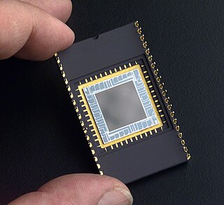
A charge-coupled device (CCD) is an integrated circuit containing an array of linked, or coupled, capacitors. Under the control of an external circuit, each capacitor can transfer its electric charge to a neighboring capacitor. CCD sensors are a major technology used in digital imaging.
In digital imaging, a pixel, pel, or picture element is the smallest addressable element in a raster image, or the smallest addressable element in a dot matrix display device. In most digital display devices, pixels are the smallest element that can be manipulated through software.

Halftone is the reprographic technique that simulates continuous-tone imagery through the use of dots, varying either in size or in spacing, thus generating a gradient-like effect. "Halftone" can also be used to refer specifically to the image that is produced by this process.
In digital signal processing, spatial anti-aliasing is a technique for minimizing the distortion artifacts (aliasing) when representing a high-resolution image at a lower resolution. Anti-aliasing is used in digital photography, computer graphics, digital audio, and many other applications.
Microscope image processing is a broad term that covers the use of digital image processing techniques to process, analyze and present images obtained from a microscope. Such processing is now commonplace in a number of diverse fields such as medicine, biological research, cancer research, drug testing, metallurgy, etc. A number of manufacturers of microscopes now specifically design in features that allow the microscopes to interface to an image processing system.
The Foveon X3 sensor is a digital camera image sensor designed by Foveon, Inc., and manufactured by Dongbu Electronics. It uses an array of photosites that consist of three vertically stacked photodiodes. Each of the three stacked photodiodes has a different spectral sensitivity, allowing it to respond differently to different wavelengths. The signals from the three photodiodes are then processed as additive color data that are transformed to a standard RGB color space.

A Bayer filter mosaic is a color filter array (CFA) for arranging RGB color filters on a square grid of photosensors. Its particular arrangement of color filters is used in most single-chip digital image sensors used in digital cameras, camcorders, and scanners to create a color image. The filter pattern is half green, one quarter red and one quarter blue, hence is also called BGGR,RGBG, GRBG, or RGGB.
Image resolution is the level of detail an image holds. The term applies to digital images, film images, and other types of images. "Higher resolution" means more image detail. Image resolution can be measured in various ways. Resolution quantifies how close lines can be to each other and still be visibly resolved. Resolution units can be tied to physical sizes, to the overall size of a picture, or to angular subtense. Instead of single lines, line pairs are often used, composed of a dark line and an adjacent light line; for example, a resolution of 10 lines per millimeter means 5 dark lines alternating with 5 light lines, or 5 line pairs per millimeter. Photographic lens and are most often quoted in line pairs per millimeter.

Super CCD is a proprietary charge-coupled device that has been developed by Fujifilm since 1999. The Super CCD uses octagonal, rather than rectangular, pixels. This allows a higher horizontal and vertical resolution to be achieved than a traditional sensor of an equivalent pixel count.
A demosaicing algorithm is a digital image process used to reconstruct a full color image from the incomplete color samples output from an image sensor overlaid with a color filter array (CFA). It is also known as CFA interpolation or color reconstruction.

Digital photography uses cameras containing arrays of electronic photodetectors interfaced to an analog-to-digital converter (ADC) to produce images focused by a lens, as opposed to an exposure on photographic film. The digitized image is stored as a computer file ready for further digital processing, viewing, electronic publishing, or digital printing. It is a form of digital imaging based on gathering visible light.

An image sensor or imager is a sensor that detects and conveys information used to form an image. It does so by converting the variable attenuation of light waves into signals, small bursts of current that convey the information. The waves can be light or other electromagnetic radiation. Image sensors are used in electronic imaging devices of both analog and digital types, which include digital cameras, camera modules, camera phones, optical mouse devices, medical imaging equipment, night vision equipment such as thermal imaging devices, radar, sonar, and others. As technology changes, electronic and digital imaging tends to replace chemical and analog imaging.

The optical transfer function (OTF) of an optical system such as a camera, microscope, human eye, or projector specifies how different spatial frequencies are captured or transmitted. It is used by optical engineers to describe how the optics project light from the object or scene onto a photographic film, detector array, retina, screen, or simply the next item in the optical transmission chain. A variant, the modulation transfer function (MTF), neglects phase effects, but is equivalent to the OTF in many situations.

An active-pixel sensor (APS) is an image sensor, which was invented by Peter J.W. Noble in 1968, where each pixel sensor unit cell has a photodetector and one or more active transistors. In a metal–oxide–semiconductor (MOS) active-pixel sensor, MOS field-effect transistors (MOSFETs) are used as amplifiers. There are different types of APS, including the early NMOS APS and the now much more common complementary MOS (CMOS) APS, also known as the CMOS sensor. CMOS sensors are used in digital camera technologies such as cell phone cameras, web cameras, most modern digital pocket cameras, most digital single-lens reflex cameras (DSLRs), mirrorless interchangeable-lens cameras (MILCs), and lensless imaging for cells.

Medipix is a family of photon counting and particle tracking pixel detectors developed by an international collaboration, hosted by CERN.
Data binning, also called data discrete binning or data bucketing, is a data pre-processing technique used to reduce the effects of minor observation errors. The original data values which fall into a given small interval, a bin, are replaced by a value representative of that interval, often a central value. It is related to quantization: data binning operates on the abscissa axis while quantization operates on the ordinate axis. Binning is a generalization of rounding.

The Nokia 808 PureView is a Symbian-powered smartphone first unveiled on 27 February 2012 at the Mobile World Congress. It is the first smartphone to feature Nokia's PureView Pro technology, a pixel oversampling technique that reduces an image taken at full resolution into a lower resolution picture, thus achieving higher definition and light sensitivity, and enables lossless digital zoom. It was one of the most advanced camera phones at the time of its release in May 2012.

The Photron FASTCAM Ultima 40K is a 256 x 256 High-speed camera. It is part of the Photron FASTCAM line of cameras, introduced in 1996. Photron FASTCAM Ultima 40K was introduce in 2000. However, the camera was trade branded previously in 1992 as a KODAK MASD product. The Kodak HS4540 and the Photron Ultima 40K are the same camera, just different trade names.

The Photron FASTCAM SE is a 256 x 256 High-speed camera. It is part of the Photron FASTCAM line of cameras, introduced in 1996. Photron FASTCAM SE was introduce in 2000. However, the camera was trade branded previously in 1992 as a KODAK MASD product. The Kodak HS4540 and the Photron SE are the same camera, just different trade names.
The Photron FASTCAM SPECTRA is a 256 x 256 High-speed camera coupled with an image intensifier. The image intensifier can shutter to 20 nanoseconds and has a spectral response between 180 nm to 800 nm. It is part of the Photron FASTCAM line of cameras, introduced in 1998.
References
- ↑ "Small explanation of binning in image processing". Steve Cannistra. Retrieved 2011-01-18.
- ↑ Bin..., ImageJ reference manual.
| | This signal processing-related article is a stub. You can help Wikipedia by expanding it. |