Power semiconductor device

Last updated

A power semiconductor device is a semiconductor device used as a switch or rectifier in power electronics (for example in a switch-mode power supply). Such a device is also called a power device or, when used in an integrated circuit, a power IC.

Contents

A power semiconductor device is usually used in "commutation mode" (i.e., it is either on or off), and therefore has a design optimized for such usage; it should usually not be used in linear operation. Linear power circuits are widespread as voltage regulators, audio amplifiers, and radio frequency amplifiers.

Power semiconductors are found in systems delivering as little as a few tens of milliwatts for a headphone amplifier, up to around a gigawatt in a high voltage direct current transmission line.

History

The first electronic device used in power circuits was the electrolytic rectifier - an early version was described by a French experimenter, A. Nodon, in 1904. These were briefly popular with early radio experimenters as they could be improvised from aluminum sheets, and household chemicals. They had low withstand voltages and limited efficiency. [1]

The first solid-state power semiconductor devices were copper oxide rectifiers, used in early battery chargers and power supplies for radio equipment, announced in 1927 by L.O. Grundahl and P. H. Geiger. [2]

The first germanium power semiconductor device appeared in 1952 with the introduction of the power diode by R.N. Hall. It had a reverse voltage blocking capability of 200 V and a current rating of 35 A.

Germanium bipolar transistors with substantial power handling capabilities (100 mA collector current) were introduced around 1952; with essentially the same construction as signal devices, but better heat sinking. Power handling capability evolved rapidly, and by 1954 germanium alloy junction transistors with 100 watt dissipation were available. These were all relatively low-frequency devices, used up to around 100 kHz, and up to 85 degrees Celsius junction temperature. [3] Silicon power transistors were not made until 1957, but when available had better frequency response than germanium devices, and could operate up to 150 C junction temperature.

The thyristor appeared in 1957. It is able to withstand very high reverse breakdown voltage and is also capable of carrying high current. However, one disadvantage of the thyristor in switching circuits is that once it becomes 'latched-on' in the conducting state; it cannot be turned off by external control, as the thyristor turn-off is passive, i.e., the power must be disconnected from the device. Thyristors which could be turned off, called gate turn-off thyristors (GTO), were introduced in 1960. [4] These overcome some limitations of the ordinary thyristor, because they can be turned on or off with an applied signal.

Power MOSFET

A breakthrough in power electronics came with the invention of the MOSFET (metal–oxide–semiconductor field-effect transistor) by Mohamed Atalla and Dawon Kahng at Bell Labs in 1959. Generations of MOSFET transistors enabled power designers to achieve performance and density levels not possible with bipolar transistors. [5] Due to improvements in MOSFET technology (initially used to produce integrated circuits), the power MOSFET became available in the 1970s.

In 1969, Hitachi introduced the first vertical power MOSFET, [6] which would later be known as the VMOS (V-groove MOSFET). [7] From 1974, Yamaha, JVC, Pioneer Corporation, Sony and Toshiba began manufacturing audio amplifiers with power MOSFETs. [8] International Rectifier introduced a 25 A, 400 V power MOSFET in 1978. [9] This device allows operation at higher frequencies than a bipolar transistor, but is limited to low voltage applications.

The Insulated-gate bipolar transistor (IGBT) was developed in the 1980s, and became widely available in the 1990s. This component has the power handling capability of the bipolar transistor and the advantages of the isolated gate drive of the power MOSFET.

Common devices

Some common power devices are the power MOSFET, power diode, thyristor, and IGBT. The power diode and power MOSFET operate on similar principles to their low-power counterparts, but are able to carry a larger amount of current and are typically able to withstand a larger reverse-bias voltage in the off-state.

Structural changes are often made in a power device in order to accommodate the higher current density, higher power dissipation, and/or higher reverse breakdown voltage. The vast majority of the discrete (i.e., non-integrated) power devices are built using a vertical structure, whereas small-signal devices employ a lateral structure. With the vertical structure, the current rating of the device is proportional to its area, and the voltage blocking capability is achieved in the height of the die. With this structure, one of the connections of the device is located on the bottom of the semiconductor die.

The power MOSFET is the most common power device in the world, due to its low gate drive power, fast switching speed, and advanced paralleling capability. [10] It has a wide range of power electronic applications, such as portable information appliances, power integrated circuits, cell phones, notebook computers, and the communications infrastructure that enables the Internet. [11] As of 2010, the power MOSFET accounts for the majority (53%) of the power transistor market, followed by the IGBT (27%), then the RF amplifier (11%), and then the bipolar junction transistor (9%). [12]

Solid-state devices

DeviceDescriptionRatings
Diode Uni-polar, uncontrolled, switching device used in applications such as rectification and circuit directional current control. Reverse voltage blocking device, commonly modeled as a switch in series with a voltage source, usually 0.7 VDC. The model can be enhanced to include a junction resistance, in order to accurately predict the diode voltage drop across the diode with respect to current flow.Up to 3000 amperes and 5000 volts in a single silicon device. High voltage requires multiple series silicon devices.
Silicon-controlled rectifier (SCR)This semi-controlled device turns on when a gate pulse is present and the anode is positive compared to the cathode. When a gate pulse is present, the device operates like a standard diode. When the anode is negative compared to the cathode, the device turns off and blocks positive or negative voltages present. The gate voltage does not allow the device to turn off. [13] Up to 3000 amperes, 5000 volts in a single silicon device.
Thyristor The thyristor is a family of three-terminal devices that include SCRs, GTOs, and MCT. For most of the devices, a gate pulse turns the device on. The device turns off when the anode voltage falls below a value (relative to the cathode) determined by the device characteristics. When off, it is considered a reverse voltage blocking device. [13]
Gate turn-off thyristor (GTO)The gate turn-off thyristor, unlike an SCR, can be turned on and off with a gate pulse. One issue with the device is that turn off gate voltages are usually larger and require more current than turn on levels. This turn off voltage is a negative voltage from gate to source, usually it only needs to be present for a short time, but the magnitude s on the order of 1/3 of the anode current. A snubber circuit is required in order to provide a usable switching curve for this device. Without the snubber circuit, the GTO cannot be used for turning inductive loads off. These devices, because of developments in IGCT technology are not very popular in the power electronics realm. They are considered controlled, uni-polar and bi-polar voltage blocking. [14]
Triac The triac is a device that is essentially an integrated pair of phase-controlled thyristors connected in inverse-parallel on the same chip. [15] Like an SCR, when a voltage pulse is present on the gate terminal, the device turns on. The main difference between an SCR and a Triac is that both the positive and negative cycle can be turned on independently of each other, using a positive or negative gate pulse. Similar to an SCR, once the device is turned on, the device cannot be turned off. This device is considered bi-polar and reverse voltage blocking.
Bipolar junction transistor (BJT)The BJT cannot be used at high power; they are slower and have more resistive losses when compared to MOSFET type devices. To carry high current, BJTs must have relatively large base currents, thus these devices have high power losses when compared to MOSFET devices. BJTs along with MOSFETs, are also considered unipolar[ clarify ] and do not block reverse voltage very well, unless installed in pairs with protection diodes. Generally, BJTs are not utilized in power electronics switching circuits because of the I2R losses associated with on resistance and base current requirements. [13] BJTs have lower current gains in high power packages, thus requiring them to be set up in Darlington configurations in order to handle the currents required by power electronic circuits. Because of these multiple transistor configurations, switching times are in the hundreds of nanoseconds to microseconds. Devices have voltage ratings which max out around 1500 V and fairly high current ratings. They can also be paralleled in order to increase power handling, but must be limited to around 5 devices for current sharing. [14]
Power MOSFET The main benefit of the power MOSFET compared to the BJT is that the MOSFET is a depletion channel device and so voltage, not current, is necessary to create a conduction path from drain to source. At low frequencies this greatly reduces gate current because it is only required to charge gate capacitance during switching, though as frequencies increase this advantage is reduced. Most losses in MOSFETs are due to on-resistance, can increase as more current flows through the device and are also greater in devices that must provide a high blocking voltage. BVdss.

Switching times range from tens of nanoseconds to a few hundred microseconds. Nominal voltages for MOSFET switching devices range from a few volts to a little over 1000 V, with currents up to about 100 A or so, though MOSFETs can be paralleled to increase switching current. MOSFET devices are not bi-directional, nor are they reverse voltage blocking. [14]

Insulated-gate bipolar transistor (IGBT)These devices have the best characteristics of MOSFETs and BJTs. Like MOSFET devices, the insulated gate bipolar transistor has a high gate impedance, thus low gate current requirements. Like BJTs, this device has low on state voltage drop, thus low power loss across the switch in operating mode. Similar to the GTO, the IGBT can be used to block both positive and negative voltages. Operating currents are fairly high, in excess of 1500 A and switching voltage up to 3000 V. [14] The IGBT has reduced input capacitance compared to MOSFET devices which improves the Miller feedback effect during high dv/dt turn on and turn off. [15]
MOS-controlled thyristor (MCT)The MOS-controlled thyristor is thyristor like and can be triggered on or off by a pulse to the MOSFET gate. [15] Since the input is MOS technology, there is very little current flow, allowing for very low power control signals. The device is constructed with two MOSFET inputs and a pair of BJT output stages. Input MOSFETs are configured to allow turn on control during positive and negative half cycles. The output BJTs are configured to allow for bidirectional control and low voltage reverse blocking. Some benefits to the MCT are fast switching frequencies, fairly high voltage and medium current ratings (around 100 A or so).
Integrated gate-commutated thyristor (IGCT)Similar to a GTO, but without the high current requirements to turn on or off the load. The IGCT can be used for quick switching with little gate current. The devices high input impedance largely because of the MOSFET gate drivers. They have low resistance outputs that do not waste power and very fast transient times that rival that of BJTs. ABB Group company has published data sheets for these devices and provided descriptions of the inner workings. The device consists of a gate, with an optically isolated input, low on resistance BJT output transistors which lead to a low voltage drop and low power loss across the device at fairly high switching voltage and current levels.

An example of this new device from ABB shows how this device improves on GTO technology for switching high voltage and high current in power electronics applications. According to ABB, the IGCT devices are capable of switching in excess of 5000 VAC and 5000 A at very high frequencies, something not possible to do efficiently with GTO devices. [16]

Classifications

Fig. 1: The power devices family, showing the principal power switches. Power devices family.png
Fig. 1: The power devices family, showing the principal power switches.

A power device may be classified as one of the following main categories (see figure 1):

Another classification is less obvious, but has a strong influence on device performance:

A majority carrier device is faster, but the charge injection of minority carrier devices allows for better on-state performance.
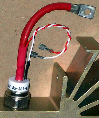
Diodes

An ideal diode should have the following characteristics:

In reality, the design of a diode is a trade-off between performance in on-state, off-state, and commutation. Indeed, the same area of the device must sustain the blocking voltage in the off-state and allow current flow in the on-state; as the requirements for the two states are completely opposite, a diode has to be either optimised for one of them, or time must be allowed to switch from one state to the other (i.e., the commutation speed must be reduced).

These trade-offs are the same for all power devices; for instance, a Schottky diode has excellent switching speed and on-state performance, but a high level of leakage current in the off-state. On the other hand, a PIN diode is commercially available in different commutation speeds (what are called "fast" and "ultrafast" rectifiers), but any increase in speed is necessarily associated with a lower performance in the on-state.

Switches

Fig.2 : Current/Voltage/switching frequency domains of the main power electronics switches. Switches domain.svg
Fig.2 : Current/Voltage/switching frequency domains of the main power electronics switches.

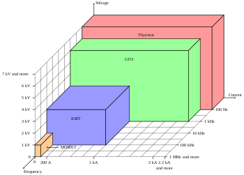
The trade-offs between voltage, current, and frequency ratings also exist for a switch. In fact, any power semiconductor relies on a PIN diode structure in order to sustain voltage; this can be seen in figure 2. The power MOSFET has the advantages of a majority carrier device, so it can achieve a very high operating frequency, but it cannot be used with high voltages; as it is a physical limit, no improvement is expected in the design of a silicon MOSFET concerning its maximum voltage ratings. However, its excellent performance in low voltage applications make it the device of choice (actually the only choice, currently) for applications with voltages below 200 V. By placing several devices in parallel, it is possible to increase the current rating of a switch. The MOSFET is particularly suited to this configuration, because its positive thermal coefficient of resistance tends to result in a balance of current between the individual devices.

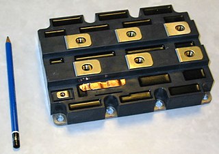
The IGBT is a recent component, so its performance improves regularly as technology evolves. It has already completely replaced the bipolar transistor in power applications; a power module is available in which several IGBT devices are connected in parallel, making it attractive for power levels up to several megawatts, which pushes further the limit at which thyristors and GTOs become the only option. Basically, an IGBT is a bipolar transistor driven by a power MOSFET; it has the advantages of being a minority carrier device (good performance in the on-state, even for high voltage devices), with the high input impedance of a MOSFET (it can be driven on or off with a very low amount of power).

The major limitation of the IGBT for low voltage applications is the high voltage drop it exhibits in the on-state (2-to-4 V). Compared to the MOSFET, the operating frequency of the IGBT is relatively low (usually not higher than 50 kHz), mainly because of a problem during turn-off known as current-tail: The slow decay of the conduction current during turn-off results from a slow recombination of a large number of carriers that flood the thick 'drift' region of the IGBT during conduction. The net result is that the turn-off switching loss  [ de ] of an IGBT is considerably higher than its turn-on loss. Generally, in datasheets, turn-off energy is mentioned as a measured parameter; that number has to be multiplied with the switching frequency of the intended application in order to estimate the turn-off loss.

At very high power levels, a thyristor-based device (e.g., a SCR, a GTO, a MCT, etc.) is still often used. This device can be turned on by a pulse provided by a driving circuit, but cannot be turned off by removing the pulse. A thyristor turns off as soon as no more current flows through it; this happens automatically in an alternating current system on each cycle, or requires a circuit with the means to divert current around the device. Both MCTs and GTOs have been developed to overcome this limitation, and are widely used in power distribution applications.

A few applications of power semiconductors in switch mode include lamp dimmers, switch mode power supplies, induction cookers, automotive ignition systems, and AC and DC electric motor drives of all sizes.

Amplifiers

Amplifiers operate in the active region, where both device current and voltage are non-zero. Consequently power is continually dissipated and its design is dominated by the need to remove excess heat from the semiconductor device. Power amplifier devices can often be recognized by the heat sink used to mount the devices. Multiple types of power semiconductor amplifier device exist, such as the bipolar junction transistor, the vertical MOS field effect transistor, and others. Power levels for individual amplifier devices range up to hundreds of watts, and frequency limits range up to the lower microwave bands. A complete audio power amplifier, with two channels and a power rating on the order of tens of watts, can be put into a small integrated circuit package, needing only a few external passive components to function. Another important application for active-mode amplifiers is in linear regulated power supplies, when an amplifier device is used as a voltage regulator to maintain load voltage at a desired setting. While such a power supply may be less energy efficient than a switched mode power supply, the simplicity of application makes them popular, especially in current ranges up to about one amp.

Parameters

A power device is usually attached to a heatsink to remove the heat caused by operation losses. Thermal stack.svg
A power device is usually attached to a heatsink to remove the heat caused by operation losses.
The power semiconductor die of a three-terminal device (IGBT, MOSFET or BJT). Two contacts are on top of the die, the remaining one is on the back. Power die.svg
The power semiconductor die of a three-terminal device (IGBT, MOSFET or BJT). Two contacts are on top of the die, the remaining one is on the back.
  1. Breakdown voltage: Often, there is a trade-off between breakdown voltage rating and on-resistance, because increasing the breakdown voltage by incorporating a thicker and lower doped drift region leads to a higher on-resistance.
  2. On-resistance: A higher current rating lowers the on-resistance due to greater numbers of parallel cells. This increases overall capacitance and slows down the speed.
  3. Rise and fall times: The amount of time it takes to switch between the on-state and the off-state.
  4. Safe-operating area: This is a thermal dissipation and "latch-up" consideration.
  5. Thermal resistance: This is an often ignored but extremely important parameter from the point of view of practical design; a semiconductor does not perform well at elevated temperature, and yet due to large current conduction, a power semiconductor device invariably heats up. Therefore, such a devices needs to be cooled by removing that heat continuously; packaging and heatsink technology provide a means for removing heat from a semiconductor device by conducting it to the external environment. Generally, a large current device has a large die and packaging surface areas and lower thermal resistance.

Research and development

Packaging

The role of packaging is to:

Many of the reliability issues of a power device are either related to excessive temperature or fatigue due to thermal cycling. Research is currently carried out on the following topics:

Research is also ongoing on electrical issues such as reducing the parasitic inductance of packaging; this inductance limits the operating frequency, because it generates losses during commutation.

A low-voltage MOSFET is also limited by the parasitic resistance of its package, as its intrinsic on-state resistance is as low as one or two milliohms.

Some of the most common type of power semiconductor packages include the TO-220, TO-247, TO-262, TO-3, D2Pak, etc.

Improvement of structures

The IGBT design is still under development and can be expected to provide increases in operating voltages. At the high-power end of the range, the MOS-controlled thyristor is a promising device. Achieving a major improvement over the conventional MOSFET structure by employing the super junction charge-balance principle: essentially, it allows the thick drift region of a power MOSFET to be heavily doped, thereby reducing the electrical resistance to electron flow without compromising the breakdown voltage. This is juxtaposed with a region that is similarly doped with the opposite carrier polarity (holes); these two similar, but oppositely doped regions effectively cancel out their mobile charge and develop a 'depleted region' that supports the high voltage during the off-state. On the other hand, during the on-state, the higher doping of the drift region allows for the easy flow of carriers, thereby reducing on-resistance. Commercial devices, based on this super junction principle, have been developed by companies like Infineon (CoolMOS products) and International Rectifier (IR).

Wide band-gap semiconductors

The major breakthrough in power semiconductor devices is expected from the replacement of silicon by a wide band-gap semiconductor. At the moment, silicon carbide (SiC) is considered to be the most promising. A SiC Schottky diode with a breakdown voltage of 1200 V is commercially available, as is a 1200 V JFET. As both are majority carrier devices, they can operate at high speed. A bipolar device is being developed for higher voltages (up to 20 kV). Among its advantages, silicon carbide can operate at a higher temperature (up to 400 °C) and has a lower thermal resistance than silicon, allowing for better cooling.

See also

Notes and references

Notes

  1. Bernard Finn, Exposing Electronics, CRC Press, 2000 ISBN   9058230562 pages 14-15
  2. Peter Robin Morris, A History of the World Semiconductor Industry, IET 1990 ISBN   0863412270 page 18
  3. Peter Robin Morris, A History of the World Semiconductor Industry, IET 1990 ISBN   0863412270 pages 39-41
  4. H. van Ligten, D. Navon, "Basic turn-off of GTO switches", IRE Wescon Convention Record, Part 3 on Electron Devices, pp. 49 - 52, August 1960.
  5. "Rethink Power Density with GaN". Electronic Design . 21 April 2017. Retrieved 23 July 2019.
  6. Oxner, E. S. (1988). Fet Technology and Application. CRC Press. p. 18. ISBN   9780824780500.
  7. "Advances in Discrete Semiconductors March On". Power Electronics Technology. Informa: 52–6. September 2005. Archived (PDF) from the original on 22 March 2006. Retrieved 31 July 2019.
  8. Duncan, Ben (1996). High Performance Audio Power Amplifiers. Elsevier. pp.  177-8, 406. ISBN   9780080508047.
  9. Jacques Arnould, Pierre Merle Dispositifs de l'électronique de puissance, Éditions Hermès, ISBN   2-86601-306-9 (in French)
  10. "Power MOSFET Basics" (PDF). Alpha & Omega Semiconductor. Retrieved 29 July 2019.
  11. Whiteley, Carol; McLaughlin, John Robert (2002). Technology, Entrepreneurs, and Silicon Valley. Institute for the History of Technology. ISBN   9780964921719. These active electronic components, or power semiconductor products, from Siliconix are used to switch and convert power in a wide range of systems, from portable information appliances to the communications infrastructure that enables the Internet. The company's power MOSFETs — tiny solid-state switches, or metal oxide semiconductor field-effect transistors — and power integrated circuits are widely used in cell phones and notebook computers to manage battery power efficiently
  12. "Power Transistor Market Will Cross $13.0 Billion in 2011". IC Insights. June 21, 2011. Retrieved 15 October 2019.
  13. 1 2 3 Hart, D. (2010). Power Electronics. McGraw-Hill Education. pp. Chapter 1. ISBN   978-0-07-128930-6.
  14. 1 2 3 4 Mohan, N. (2003). Power Electronics Converters Applications and Design. Michigan: John Wiley and Sons. pp. Chapter 1. ISBN   978-0-471-22693-2.
  15. 1 2 3 Bose, B (April 1992). "Evaluation of Modern Power Semiconductor Devices and Future Trends of Converters". IEEE Transactions on Industry Applications. 28 (2): 403–413. doi:10.1109/28.126749. S2CID   14387438.
  16. "semiconductor GTO". GTO. ABB. Retrieved 21 March 2012.
  17. Robert Boylestad and Louis Nashelsky (2006). Electronic Devices. and Circuit Theory. 9th edition Prentice Hall. Upper Saddle River, New Jersey. Columbus

Related Research Articles

<span class="mw-page-title-main">Transistor</span> Solid-state electrically operated switch also used as an amplifier

A transistor is a semiconductor device used to amplify or switch electrical signals and power. It is one of the basic building blocks of modern electronics. It is composed of semiconductor material, usually with at least three terminals for connection to an electronic circuit. A voltage or current applied to one pair of the transistor's terminals controls the current through another pair of terminals. Because the controlled (output) power can be higher than the controlling (input) power, a transistor can amplify a signal. Some transistors are packaged individually, but many more in miniature form are found embedded in integrated circuits. Because transistors are the key active components in practically all modern electronics, many people consider them one of the 20th century's greatest inventions.

<span class="mw-page-title-main">Semiconductor device</span> Electronic component that exploits the electronic properties of semiconductor materials

A semiconductor device is an electronic component that relies on the electronic properties of a semiconductor material for its function. Its conductivity lies between conductors and insulators. Semiconductor devices have replaced vacuum tubes in most applications. They conduct electric current in the solid state, rather than as free electrons across a vacuum or as free electrons and ions through an ionized gas.

<span class="mw-page-title-main">Insulated-gate bipolar transistor</span> Type of solid state switch

An insulated-gate bipolar transistor (IGBT) is a three-terminal power semiconductor device primarily forming an electronic switch. It was developed to combine high efficiency with fast switching. It consists of four alternating layers (P–N–P–N) that are controlled by a metal–oxide–semiconductor (MOS) gate structure.

<span class="mw-page-title-main">Thyristor</span> Type of solid state switch

A thyristor is a solid-state semiconductor device with four layers of alternating P- and N-type materials used for high-power applications. It acts as a bistable switch. There are two designs, differing in what triggers the conducting state. In a three-lead thyristor, a small current on its gate lead controls the larger current of the anode-to-cathode path. In a two-lead thyristor, conduction begins when the potential difference between the anode and cathode themselves is sufficiently large. The thyristor continues conducting until the voltage across the device is reverse-biased or the voltage is removed, or through the control gate signal on newer types.

<span class="mw-page-title-main">Schottky diode</span> Semiconductor diode

The Schottky diode, also known as Schottky barrier diode or hot-carrier diode, is a semiconductor diode formed by the junction of a semiconductor with a metal. It has a low forward voltage drop and a very fast switching action. The cat's-whisker detectors used in the early days of wireless and metal rectifiers used in early power applications can be considered primitive Schottky diodes.

<span class="mw-page-title-main">Silicon controlled rectifier</span> Four-layer solid-state current-controlling device

A silicon controlled rectifier or semiconductor controlled rectifier is a four-layer solid-state current-controlling device. The name "silicon controlled rectifier" is General Electric's trade name for a type of thyristor. The principle of four-layer p–n–p–n switching was developed by Moll, Tanenbaum, Goldey, and Holonyak of Bell Laboratories in 1956. The practical demonstration of silicon controlled switching and detailed theoretical behavior of a device in agreement with the experimental results was presented by Dr Ian M. Mackintosh of Bell Laboratories in January 1958. The SCR was developed by a team of power engineers led by Gordon Hall and commercialized by Frank W. "Bill" Gutzwiller in 1957.

<span class="mw-page-title-main">TRIAC</span> Solid-state semiconductor device

A TRIAC is a three-terminal electronic component that conducts current in either direction when triggered. The term TRIAC is a genericised trademark.

<span class="mw-page-title-main">Integrated gate-commutated thyristor</span> Power semiconductor electronic device

The integrated gate-commutated thyristor (IGCT) is a power semiconductor electronic device, used for switching electric current in industrial equipment. It is related to the gate turn-off (GTO) thyristor.

<span class="mw-page-title-main">Safe operating area</span> Technical specification

For power semiconductor devices, the safe operating area (SOA) is defined as the voltage and current conditions over which the device can be expected to operate without self-damage.

<span class="mw-page-title-main">Power electronics</span> Technology of power electronics

Power electronics is the application of electronics to the control and conversion of electric power.

<span class="mw-page-title-main">Electronic component</span> Discrete device in an electronic system

An electronic component is any basic discrete electronic device or physical entity part of an electronic system used to affect electrons or their associated fields. Electronic components are mostly industrial products, available in a singular form and are not to be confused with electrical elements, which are conceptual abstractions representing idealized electronic components and elements. A datasheet for an electronic component is a technical document that provides detailed information about the component's specifications, characteristics, and performance.

<span class="mw-page-title-main">Power MOSFET</span> MOSFET that can handle significant power levels

A power MOSFET is a specific type of metal–oxide–semiconductor field-effect transistor (MOSFET) designed to handle significant power levels. Compared to the other power semiconductor devices, such as an insulated-gate bipolar transistor (IGBT) or a thyristor, its main advantages are high switching speed and good efficiency at low voltages. It shares with the IGBT an isolated gate that makes it easy to drive. They can be subject to low gain, sometimes to a degree that the gate voltage needs to be higher than the voltage under control.

<span class="mw-page-title-main">Solid-state relay</span> High-power solid-state electronic switching device responding to an external control signal

A solid state relay (SSR) is an electronic switching device that switches on or off when an external voltage is applied across its control terminals. They serve the same function as an electromechanical relay, but solid-state electronics contain no moving parts and have a longer operational lifetime. Solid state relays were invented in 1971 by the Crydom Controls division of International Rectifiers.

<span class="mw-page-title-main">Gate turn-off thyristor</span> Semiconductor device

A gate turn-off thyristor (GTO) is a special type of thyristor, which is a high-power semiconductor device. It was invented by General Electric. GTOs, as opposed to normal thyristors, are fully controllable switches which can be turned on and off by their gate lead.

In electronics, an electronic switch is a switch controlled by an active electronic component or device. Without using moving parts, they are called solid state switches, which distinguishes them from mechanical switches.

<span class="mw-page-title-main">Shockley diode</span> Four layer semiconductor diode

The Shockley diode is a four-layer semiconductor diode, which was one of the first semiconductor devices invented. It is a PNPN diode with alternating layers of P-type and N-type material. It is equivalent to a thyristor with a disconnected gate. Shockley diodes were manufactured and marketed by Shockley Semiconductor Laboratory in the late 1950s. The Shockley diode has a negative resistance characteristic. It was largely superseded by the diac.

The current injection technique is a technique developed to reduce the turn-OFF switching transient of power bipolar semiconductor devices. It was developed and published by Dr S. Eio of Staffordshire University in 2007.

A gate driver is a power amplifier that accepts a low-power input from a controller IC and produces a high-current drive input for the gate of a high-power transistor such as an IGBT or power MOSFET. Gate drivers can be provided either on-chip or as a discrete module. In essence, a gate driver consists of a level shifter in combination with an amplifier. A gate driver IC serves as the interface between control signals and power switches. An integrated gate-driver solution reduces design complexity, development time, bill of materials (BOM), and board space while improving reliability over discretely-implemented gate-drive solutions.

The following outline is provided as an overview of and topical guide to electronics:

<span class="mw-page-title-main">Field-effect transistor</span> Type of transistor

The field-effect transistor (FET) is a type of transistor that uses an electric field to control the flow of current in a semiconductor. It comes in two types: junction FET (JFET) and metal-oxide-semiconductor FET (MOSFET). FETs have three terminals: source, gate, and drain. FETs control the flow of current by the application of a voltage to the gate, which in turn alters the conductivity between the drain and source.

References