Pulsed laser deposition

Last updated
A plume ejected from a SrRuO3 target during pulsed laser deposition. PLD Plume.png
A plume ejected from a SrRuO3 target during pulsed laser deposition.
One possible configuration of a PLD deposition chamber. Diagram of pulsed laser deposition.png
One possible configuration of a PLD deposition chamber.

Pulsed laser deposition (PLD) is a physical vapor deposition (PVD) technique where a high-power pulsed laser beam is focused inside a vacuum chamber to strike a target of the material that is to be deposited. This material is vaporized from the target (in a plasma plume) which deposits it as a thin film on a substrate (such as a silicon wafer facing the target). This process can occur in ultra high vacuum or in the presence of a background gas, such as oxygen which is commonly used when depositing oxides to fully oxygenate the deposited films.

Contents

While the basic setup is simple relative to many other deposition techniques, the physical phenomena of laser-target interaction and film growth are quite complex (see Process below). When the laser pulse is absorbed by the target, energy is first converted to electronic excitation and then into thermal, chemical and mechanical energy resulting in evaporation, ablation, plasma formation and even exfoliation. [1] The ejected species expand into the surrounding vacuum in the form of a plume containing many energetic species including atoms, molecules, electrons, ions, clusters, particulates and molten globules, before depositing on the typically hot substrate.

Process

The detailed mechanisms of PLD are very complex including the ablation process of the target material by the laser irradiation, the development of a plasma plume with high energetic ions, electrons as well as neutrals and the crystalline growth of the film itself on the heated substrate. The process of PLD can generally be divided into four stages:

Each of these steps is crucial for the crystallinity, uniformity and stoichiometry of the resulting film. The most used methods for modelling the PLD process are the Monte Carlo techniques. [2]

Thin films of oxides are deposited with atomic layer precision using pulsed laser deposition. In this picture, a high-intensity pulsed laser shoots a rotating white disk of Al2O3 (alumina). The laser pulse creates a plasma explosion, visible as the purple cloud. The plasma cloud from the alumina expands towards the square substrate, made of SrTiO3, where it condenses and solidifies, building up one atomic layer at a time. The substrate is mounted on a heating plate, glowing red at a temperature of 650 degC, to improve the crystallinity of the alumina thin film. Pulsed Laser Deposition in Action.jpg
Thin films of oxides are deposited with atomic layer precision using pulsed laser deposition. In this picture, a high-intensity pulsed laser shoots a rotating white disk of Al2O3 (alumina). The laser pulse creates a plasma explosion, visible as the purple cloud. The plasma cloud from the alumina expands towards the square substrate, made of SrTiO3, where it condenses and solidifies, building up one atomic layer at a time. The substrate is mounted on a heating plate, glowing red at a temperature of 650 °C, to improve the crystallinity of the alumina thin film.

Laser ablation of the target material and creation of a plasma

The ablation of the target material upon laser irradiation and the creation of plasma are very complex processes. The removal of atoms from the bulk material is done by vaporization of the bulk at the surface region in a state of non-equilibrium. In this the incident laser pulse penetrates into the surface of the material within the penetration depth. This dimension is dependent on the laser wavelength and the index of refraction of the target material at the applied laser wavelength and is typically in the region of 10 nm for most materials. The strong electrical field generated by the laser light is sufficiently strong to remove the electrons from the bulk material of the penetrated volume. This process occurs within 10 ps of a ns laser pulse and is caused by non-linear processes such as multiphoton ionization which are enhanced by microscopic cracks at the surface, voids, and nodules, which increase the electric field. The free electrons oscillate within the electromagnetic field of the laser light and can collide with the atoms of the bulk material thus transferring some of their energy to the lattice of the target material within the surface region. The surface of the target is then heated up and the material is vaporized.

Dynamic of the plasma

In the second stage the material expands in a plasma parallel to the normal vector of the target surface towards the substrate due to Coulomb repulsion and recoil from the target surface. The spatial distribution of the plume is dependent on the background pressure inside the PLD chamber. The density of the plume can be described by a cosn(x) law with a shape similar to a Gaussian curve. The dependency of the plume shape on the pressure can be described in three stages:

The most important consequence of increasing the background pressure is the slowing down of the high energetic species in the expanding plasma plume. It has been shown that particles with kinetic energies around 50 eV can resputter the film already deposited on the substrate. This results in a lower deposition rate and can furthermore result in a change in the stoichiometry of the film.

Deposition of the ablation material on the substrate

The third stage is important to determine the quality of the deposited films. The high energetic species ablated from the target are bombarding the substrate surface and may cause damage to the surface by sputtering off atoms from the surface but also by causing defect formation in the deposited film. [3] The sputtered species from the substrate and the particles emitted from the target form a collision region, which serves as a source for condensation of particles. When the condensation rate is high enough, a thermal equilibrium can be reached and the film grows on the substrate surface at the expense of the direct flow of ablation particles and the thermal equilibrium obtained.

Nucleation and growth of the film on the substrate surface

The nucleation process and growth kinetics of the film depend on several growth parameters including:

In PLD, a large supersaturation occurs on the substrate during the pulse duration. The pulse lasts around 10–40 microseconds [9] depending on the laser parameters. This high supersaturation causes a very large nucleation density on the surface as compared to molecular beam epitaxy or sputtering deposition. This nucleation density increases the smoothness of the deposited film.

In PLD, [depending on the deposition parameters above] three growth modes are possible:

History

Pulsed laser deposition is only one of many thin film deposition techniques. Other methods include molecular beam epitaxy (MBE), chemical vapor deposition (CVD), sputter deposition (RF, magnetron, and ion beam). The history of laser-assisted film growth started soon after the technical realization of the first laser in 1960 by Maiman. Smith and Turner utilized a ruby laser to deposit the first thin films in 1965, three years after Breech and Cross studied the laser-vaporization and excitation of atoms from solid surfaces. However, the deposited films were still inferior to those obtained by other techniques such as chemical vapor deposition and molecular beam epitaxy. In the early 1980s, a few research groups (mainly in the former USSR) achieved remarkable results on manufacturing of thin film structures utilizing laser technology. The breakthrough came in 1987 when D. Dijkkamp, Xindi Wu and T. Venkatesan were able to laser deposit a thin film of YBa2Cu3O7, a high temperature superconductive material, which was of superior quality to that of films deposited with alternative techniques. Since then, the technique of pulsed laser deposition has been utilized to fabricate high quality crystalline films, such as doped garnet thin films for use as planar waveguide lasers. [11] [12] The deposition of ceramic oxides, [13] nitride films, [14] ferromagnetic films, [15] metallic multilayers [16] [17] and various superlattices has been demonstrated. In the 1990s the development of new laser technology, such as lasers with high repetition rate and short pulse durations, made PLD a very competitive tool for the growth of thin, well defined films with complex stoichiometry.

Technical aspects

There are many different arrangements to build a deposition chamber for PLD. The target material which is evaporated by the laser is normally found as a rotating disc attached to a support. However, it can also be sintered into a cylindrical rod with rotational motion and a translational up and down movement along its axis. This special configuration allows not only the utilization of a synchronized reactive gas pulse but also of a multicomponent target rod with which films of different multilayers can be created.

Some factors that influence the deposition rate:

Related Research Articles

<span class="mw-page-title-main">Chemical vapor deposition</span> Method used to apply surface coatings

Chemical vapor deposition (CVD) is a vacuum deposition method used to produce high-quality, and high-performance, solid materials. The process is often used in the semiconductor industry to produce thin films.

<span class="mw-page-title-main">Epitaxy</span> Crystal growth process relative to the substrate

Epitaxy refers to a type of crystal growth or material deposition in which new crystalline layers are formed with one or more well-defined orientations with respect to the crystalline seed layer. The deposited crystalline film is called an epitaxial film or epitaxial layer. The relative orientation(s) of the epitaxial layer to the seed layer is defined in terms of the orientation of the crystal lattice of each material. For most epitaxial growths, the new layer is usually crystalline and each crystallographic domain of the overlayer must have a well-defined orientation relative to the substrate crystal structure. Epitaxy can involve single-crystal structures, although grain-to-grain epitaxy has been observed in granular films. For most technological applications, single-domain epitaxy, which is the growth of an overlayer crystal with one well-defined orientation with respect to the substrate crystal, is preferred. Epitaxy can also play an important role while growing superlattice structures.

<span class="mw-page-title-main">Molecular-beam epitaxy</span> Crystal growth process

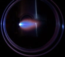
Molecular-beam epitaxy (MBE) is an epitaxy method for thin-film deposition of single crystals. MBE is widely used in the manufacture of semiconductor devices, including transistors, and it is considered one of the fundamental tools for the development of nanotechnologies. MBE is used to fabricate diodes and MOSFETs at microwave frequencies, and to manufacture the lasers used to read optical discs.

A thin film is a layer of material ranging from fractions of a nanometer (monolayer) to several micrometers in thickness. The controlled synthesis of materials as thin films is a fundamental step in many applications. A familiar example is the household mirror, which typically has a thin metal coating on the back of a sheet of glass to form a reflective interface. The process of silvering was once commonly used to produce mirrors, while more recently the metal layer is deposited using techniques such as sputtering. Advances in thin film deposition techniques during the 20th century have enabled a wide range of technological breakthroughs in areas such as magnetic recording media, electronic semiconductor devices, integrated passive devices, LEDs, optical coatings, hard coatings on cutting tools, and for both energy generation and storage. It is also being applied to pharmaceuticals, via thin-film drug delivery. A stack of thin films is called a multilayer.

Atomic layer epitaxy (ALE), more generally known as atomic layer deposition (ALD), is a specialized form of thin film growth (epitaxy) that typically deposit alternating monolayers of two elements onto a substrate. The crystal lattice structure achieved is thin, uniform, and aligned with the structure of the substrate. The reactants are brought to the substrate as alternating pulses with "dead" times in between. ALE makes use of the fact that the incoming material is bound strongly until all sites available for chemisorption are occupied. The dead times are used to flush the excess material. It is mostly used in semiconductor fabrication to grow thin films of thickness in the nanometer scale.

Chemical beam epitaxy (CBE) forms an important class of deposition techniques for semiconductor layer systems, especially III-V semiconductor systems. This form of epitaxial growth is performed in an ultrahigh vacuum system. The reactants are in the form of molecular beams of reactive gases, typically as the hydride or a metalorganic. The term CBE is often used interchangeably with metal-organic molecular beam epitaxy (MOMBE). The nomenclature does differentiate between the two processes, however. When used in the strictest sense, CBE refers to the technique in which both components are obtained from gaseous sources, while MOMBE refers to the technique in which the group III component is obtained from a gaseous source and the group V component from a solid source.

Atomic layer deposition (ALD) is a thin-film deposition technique based on the sequential use of a gas-phase chemical process; it is a subclass of chemical vapour deposition. The majority of ALD reactions use two chemicals called precursors. These precursors react with the surface of a material one at a time in a sequential, self-limiting, manner. A thin film is slowly deposited through repeated exposure to separate precursors. ALD is a key process in fabricating semiconductor devices, and part of the set of tools for synthesizing nanomaterials.

GeSbTe (germanium-antimony-tellurium or GST) is a phase-change material from the group of chalcogenide glasses used in rewritable optical discs and phase-change memory applications. Its recrystallization time is 20 nanoseconds, allowing bitrates of up to 35 Mbit/s to be written and direct overwrite capability up to 106 cycles. It is suitable for land-groove recording formats. It is often used in rewritable DVDs. New phase-change memories are possible using n-doped GeSbTe semiconductor. The melting point of the alloy is about 600 °C (900 K) and the crystallization temperature is between 100 and 150 °C.

<span class="mw-page-title-main">Physical vapor deposition</span> Method of coating solid surfaces with thin films

Physical vapor deposition (PVD), sometimes called physical vapor transport (PVT), describes a variety of vacuum deposition methods which can be used to produce thin films and coatings on substrates including metals, ceramics, glass, and polymers. PVD is characterized by a process in which the material transitions from a condensed phase to a vapor phase and then back to a thin film condensed phase. The most common PVD processes are sputtering and evaporation. PVD is used in the manufacturing of items which require thin films for optical, mechanical, electrical, acoustic or chemical functions. Examples include semiconductor devices such as thin-film solar cells, microelectromechanical devices such as thin film bulk acoustic resonator, aluminized PET film for food packaging and balloons, and titanium nitride coated cutting tools for metalworking. Besides PVD tools for fabrication, special smaller tools used mainly for scientific purposes have been developed.

Laser peening (LP), or laser shock peening (LSP), is a surface engineering process used to impart beneficial residual stresses in materials. The deep, high-magnitude compressive residual stresses induced by laser peening increase the resistance of materials to surface-related failures, such as fatigue, fretting fatigue, and stress corrosion cracking. Laser shock peening can also be used to strengthen thin sections, harden surfaces, shape or straighten parts, break up hard materials, compact powdered metals and for other applications where high-pressure, short duration shock waves offer desirable processing results.

<span class="mw-page-title-main">Sputter deposition</span> Method of thin film application

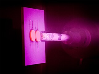
Sputter deposition is a physical vapor deposition (PVD) method of thin film deposition by the phenomenon of sputtering. This involves ejecting material from a "target" that is a source onto a "substrate" such as a silicon wafer. Resputtering is re-emission of the deposited material during the deposition process by ion or atom bombardment. Sputtered atoms ejected from the target have a wide energy distribution, typically up to tens of eV. The sputtered ions can ballistically fly from the target in straight lines and impact energetically on the substrates or vacuum chamber. Alternatively, at higher gas pressures, the ions collide with the gas atoms that act as a moderator and move diffusively, reaching the substrates or vacuum chamber wall and condensing after undergoing a random walk. The entire range from high-energy ballistic impact to low-energy thermalized motion is accessible by changing the background gas pressure. The sputtering gas is often an inert gas such as argon. For efficient momentum transfer, the atomic weight of the sputtering gas should be close to the atomic weight of the target, so for sputtering light elements neon is preferable, while for heavy elements krypton or xenon are used. Reactive gases can also be used to sputter compounds. The compound can be formed on the target surface, in-flight or on the substrate depending on the process parameters. The availability of many parameters that control sputter deposition make it a complex process, but also allow experts a large degree of control over the growth and microstructure of the film.

High-power impulse magnetron sputtering is a method for physical vapor deposition of thin films which is based on magnetron sputter deposition. HIPIMS utilises extremely high power densities of the order of kW⋅cm−2 in short pulses (impulses) of tens of microseconds at low duty cycle of < 10%. Distinguishing features of HIPIMS are a high degree of ionisation of the sputtered metal and a high rate of molecular gas dissociation which result in high density of deposited films. The ionization and dissociation degree increase according to the peak cathode power. The limit is determined by the transition of the discharge from glow to arc phase. The peak power and the duty cycle are selected so as to maintain an average cathode power similar to conventional sputtering (1–10 W⋅cm−2).

Stranski–Krastanov growth is one of the three primary modes by which thin films grow epitaxially at a crystal surface or interface. Also known as 'layer-plus-island growth', the SK mode follows a two step process: initially, complete films of adsorbates, up to several monolayers thick, grow in a layer-by-layer fashion on a crystal substrate. Beyond a critical layer thickness, which depends on strain and the chemical potential of the deposited film, growth continues through the nucleation and coalescence of adsorbate 'islands'. This growth mechanism was first noted by Ivan Stranski and Lyubomir Krastanov in 1938. It wasn't until 1958 however, in a seminal work by Ernst Bauer published in Zeitschrift für Kristallographie, that the SK, Volmer–Weber, and Frank–van der Merwe mechanisms were systematically classified as the primary thin-film growth processes. Since then, SK growth has been the subject of intense investigation, not only to better understand the complex thermodynamics and kinetics at the core of thin-film formation, but also as a route to fabricating novel nanostructures for application in the microelectronics industry.

<span class="mw-page-title-main">Vapor–liquid–solid method</span> Mechanism to grow nano wires

The vapor–liquid–solid method (VLS) is a mechanism for the growth of one-dimensional structures, such as nanowires, from chemical vapor deposition. The growth of a crystal through direct adsorption of a gas phase on to a solid surface is generally very slow. The VLS mechanism circumvents this by introducing a catalytic liquid alloy phase which can rapidly adsorb a vapor to supersaturation levels, and from which crystal growth can subsequently occur from nucleated seeds at the liquid–solid interface. The physical characteristics of nanowires grown in this manner depend, in a controllable way, upon the size and physical properties of the liquid alloy.

<span class="mw-page-title-main">Superconducting wire</span> Wires exhibiting zero resistance

Superconducting wires are electrical wires made of superconductive material. When cooled below their transition temperatures, they have zero electrical resistance. Most commonly, conventional superconductors such as niobium–titanium are used, but high-temperature superconductors such as YBCO are entering the market.

<span class="mw-page-title-main">Crystalline silicon</span> Semiconducting material used in solar cell technology

Crystalline silicon or (c-Si) Is the crystalline forms of silicon, either polycrystalline silicon, or monocrystalline silicon. Crystalline silicon is the dominant semiconducting material used in photovoltaic technology for the production of solar cells. These cells are assembled into solar panels as part of a photovoltaic system to generate solar power from sunlight.

Lanthanum aluminate is an inorganic compound with the formula LaAlO3, often abbreviated as LAO. It is an optically transparent ceramic oxide with a distorted perovskite structure.

A rapidly increasing list of graphene production techniques have been developed to enable graphene's use in commercial applications.

Molecular layer deposition (MLD) is a vapour phase thin film deposition technique based on self-limiting surface reactions carried out in a sequential manner. Essentially, MLD resembles the well established technique of atomic layer deposition (ALD) but, whereas ALD is limited to exclusively inorganic coatings, the precursor chemistry in MLD can use small, bifunctional organic molecules as well. This enables, as well as the growth of organic layers in a process similar to polymerization, the linking of both types of building blocks together in a controlled way to build up organic-inorganic hybrid materials.

<span class="mw-page-title-main">Thermal laser epitaxy</span>

Thermal laser epitaxy (TLE) is a physical vapor deposition technique that utilizes irradiation from continuous-wave lasers to heat sources locally for growing films on a substrate. This technique can be performed under ultra-high vacuum pressure or in the presence of a background atmosphere, such as ozone, to deposit oxide films.

References

  1. Pulsed Laser Deposition of Thin Films, edited by Douglas B. Chrisey and Graham K. Hubler, John Wiley & Sons, 1994 ISBN   0-471-59218-8
  2. Rashidian Vaziri, M R (2011). "Monte Carlo simulation of the subsurface growth mode during pulsed laser deposition". Journal of Applied Physics. 110 (4): 043304–043304–12. Bibcode:2011JAP...110d3304R. doi:10.1063/1.3624768.
  3. Vaziri, M R R (2010). "Microscopic description of the thermalization process during pulsed laser deposition of aluminium in the presence of argon background gas". Journal of Physics D: Applied Physics. 43 (42): 425205. Bibcode:2010JPhD...43P5205R. doi:10.1088/0022-3727/43/42/425205. S2CID   120309363.
  4. Ohnishi, Tsuyoshi; Shibuya, Keisuke; Yamamoto, Takahisa; Lippmaa, Mikk (2008). "Defects and transport in complex oxide thin films". Journal of Applied Physics. 103 (10): 103703–103703–6. Bibcode:2008JAP...103j3703O. doi:10.1063/1.2921972.
  5. Ferguson, J. D.; Arikan, G.; Dale, D. S.; Woll, A. R.; Brock, J. D. (2009). "Measurements of Surface Diffusivity and Coarsening during Pulsed Laser Deposition". Physical Review Letters. 103 (25): 256103. arXiv: 0910.3601 . Bibcode:2009PhRvL.103y6103F. doi:10.1103/PhysRevLett.103.256103. PMID   20366266. S2CID   11210950.
  6. May-Smith, T. C.; Muir, A. C.; Darby, M. S. B.; Eason, R. W. (2008-04-10). "Design and performance of a ZnSe tetra-prism for homogeneous substrate heating using a CO2 laser for pulsed laser deposition experiments" (PDF). Applied Optics. 47 (11): 1767–1780. Bibcode:2008ApOpt..47.1767M. doi:10.1364/AO.47.001767. ISSN   1539-4522. PMID   18404174.
  7. Koster, Gertjan; Kropman, Boike L.; Rijnders, Guus J. H. M.; Blank, Dave H. A.; Rogalla, Horst (1998). "Quasi-ideal strontium titanate crystal surfaces through formation of strontium hydroxide". Applied Physics Letters. 73 (20): 2920. Bibcode:1998ApPhL..73.2920K. doi:10.1063/1.122630.
  8. Ohtomo, A.; Hwang, H. Y. (2007). "Growth mode control of the free carrier density in SrTiO[sub 3−δ] films". Journal of Applied Physics. 102 (8): 083704–083704–6. arXiv: cond-mat/0604117 . Bibcode:2007JAP...102h3704O. doi:10.1063/1.2798385. S2CID   118558366.
  9. Granozio, F. M. et al. In-situ Investigation of Surface Oxygen Vacancies in Perovskites Mat. Res. Soc. Proc. 967E, (2006)
  10. Lippmaa, M.; Nakagawa, N.; Kawasaki, M.; Ohashi, S.; Koinuma, H. (2000). "Growth mode mapping of SrTiO[sub 3] epitaxy". Applied Physics Letters. 76 (17): 2439. Bibcode:2000ApPhL..76.2439L. doi:10.1063/1.126369.
  11. Grant-Jacob, James A.; Beecher, Stephen J.; Parsonage, Tina L.; Hua, Ping; Mackenzie, Jacob I.; Shepherd, David P.; Eason, Robert W. (2016-01-01). "An 115 W Yb:YAG planar waveguide laser fabricated via pulsed laser deposition" (PDF). Optical Materials Express . 6 (1): 91. Bibcode:2016OMExp...6...91G. doi: 10.1364/ome.6.000091 . ISSN   2159-3930.
  12. Beecher, Stephen J.; Grant-Jacob, James A.; Hua, Ping; Prentice, Jake J.; Eason, Robert W.; Shepherd, David P.; Mackenzie, Jacob I. (2017-05-01). "Ytterbium-doped-garnet crystal waveguide lasers grown by pulsed laser deposition". Optical Materials Express . 7 (5): 1628. Bibcode:2017OMExp...7.1628B. doi: 10.1364/OME.7.001628 . ISSN   2159-3930.
  13. Koinuma, Hideomi; Nagata, Hirotoshi; Tsukahara, Tadashi; Gonda, Satoshi; Yoshimoto, Mamoru (1991-05-06). "Ceramic layer epitaxy by pulsed laser deposition in an ultrahigh vacuum system". Applied Physics Letters. 58 (18): 2027–2029. Bibcode:1991ApPhL..58.2027K. doi:10.1063/1.105002. ISSN   0003-6951.
  14. Vispute, R. D.; Talyansky, V.; Trajanovic, Z.; Choopun, S.; Downes, M.; Sharma, R. P.; Venkatesan, T.; Woods, M. C.; Lareau, R. T. (1997-05-19). "High quality crystalline ZnO buffer layers on sapphire (001) by pulsed laser deposition for III–V nitrides". Applied Physics Letters. 70 (20): 2735–2737. Bibcode:1997ApPhL..70.2735V. doi:10.1063/1.119006. ISSN   0003-6951.
  15. Yoshitake, Tsuyoshi; Nakagauchi, Dai; Nagayama, Kunihito (2003-07-15). "Ferromagnetic Iron Silicide Thin Films Prepared by Pulsed-Laser Deposition". Japanese Journal of Applied Physics. 42 (Part 2, No. 7B): L849–L851. Bibcode:2003JaJAP..42L.849Y. doi:10.1143/JJAP.42.L849. ISSN   0021-4922. S2CID   119738424.
  16. Shen, J.; Gai, Zheng; Kirschner, J. (February 2004). "Growth and magnetism of metallic thin films and multilayers by pulsed-laser deposition". Surface Science Reports. 52 (5–6): 163–218. doi:10.1016/j.surfrep.2003.10.001.
  17. Lunney, James G. (February 1995). "Pulsed laser deposition of metal and metal multilayer films". Applied Surface Science. 86 (1–4): 79–85. Bibcode:1995ApSS...86...79L. doi:10.1016/0169-4332(94)00368-8.
  18. Grant-Jacob, James A.; Beecher, Stephen J.; Prentice, Jake J.; Shepherd, David P.; Mackenzie, Jacob I.; Eason, Robert W. (June 2018). "Pulsed laser deposition of crystalline garnet waveguides at a growth rate of 20 μm per hour". Surface and Coatings Technology. 343: 7–10. doi: 10.1016/j.surfcoat.2017.12.008 .
  19. Grant-Jacob, James A.; Beecher, Stephen J.; Riris, Haris; Yu, Anthony W.; Shepherd, David P.; Eason, Robert W.; Mackenzie, Jacob I. (23 October 2017). "Dynamic control of refractive index during pulsed-laser-deposited waveguide growth". Optical Materials Express . 7 (11): 4073. Bibcode:2017OMExp...7.4073G. doi: 10.1364/OME.7.004073 .
  20. Scharf, T.; Krebs, H.U. (1 November 2002). "Influence of inert gas pressure on deposition rate during pulsed laser deposition". Applied Physics A: Materials Science & Processing. 75 (5): 551–554. Bibcode:2002ApPhA..75..551S. doi:10.1007/s00339-002-1442-4. S2CID   93176756.