RAM limit

Last updated

The maximum random access memory (RAM) installed in any computer system is limited by hardware, software and economic factors. The hardware may have a limited number of address bus bits, limited by the processor package or design of the system. Some of the address space may be shared between RAM, peripherals, and read-only memory. In the case of a microcontroller with no external RAM, the size of the RAM array is limited by the size of the integrated circuit die. In a packaged system, only enough RAM may be provided for the system's required functions, with no provision for addition of memory after manufacture.

Contents

Software limitations to usable physical RAM may be present. An operating system may only be designed to allocate a certain amount of memory, with upper address bits reserved to indicate designations such as I/O or supervisor mode or other security information. Or the operating system may rely on internal data structures with fixed limits for addressable memory.

For mass-market personal computers, there may be no financial advantage to a manufacturer in providing more memory sockets, address lines, or other hardware than necessary to run mass-market software. When memory devices were relatively expensive compared with the processor, often the RAM delivered with the system was much less than the address capacity of the hardware, because of cost.

Sometimes RAM limits can be overcome using special techniques. Bank switching allows blocks of RAM memory to be switched into the processor's address space when required, under program control. Operating systems routinely manage running programs using virtual memory, where individual program operate as if they have access to a large memory space that is being simulated by swapping memory areas with disk storage.

CPU addressing limits

For performance reasons, all the parallel address lines of an address bus must be valid at the same time, otherwise access to memory would be delayed and performance would be seriously reduced. Integrated circuit packages may have a limit on the number of pins available to provide the memory bus. Different versions of a CPU architecture, in different-sized IC packages, can be designed, trading off reduced package size for reduced pin count and address space. A trade-off might be made between address pins and other functions, restricting the memory physically available to an architecture even if it inherently has a higher capacity. On the other hand, segmented or bank switching designs provide more memory address space than is available in an internal memory address register.

As integrated circuit memory became less costly, it was feasible to design systems with larger and larger physical memory spaces.

Fewer than 16 address pins

Microcontroller devices with integrated I/O and memory on-chip sometimes had no, or a small, address bus available for external devices. For example, a microcontroller family available with a 2 kilobyte address space might have a variant that brought out an 11 line address bus for an external ROM; this could be done by reassigning I/O pins as address bus pins. Some general-purpose processors with integrated ROM split a 16-bit address space between internal ROM and an external 15-bit memory bus.

Some microprocessors had fewer than 16 address pins: for example, the MOS Technology 6507 (a reduced pin count version of the 6502) was used in the Atari 2600 and was limited to a 13-line address bus.

16 address bits, 16 address pins

Most 8-bit general-purpose microprocessors have 16-bit address spaces and generate 16 address lines. Examples include the Intel 8080, Intel 8085, Zilog Z80, Motorola 6800, Microchip PIC18, and many others. These processors have 8-bit CPUs with 8-bit data and 16-bit addressing. The memory on these CPUs is addressable at the byte level. This leads to a memory addressable limit of 216 × 1 byte = 65,536 bytes or 64 kilobytes.

16 address bits, 20 address pins: 8086, 8088, 80186 & 80188

The Intel 8086 and derivatives, such as the 8088, 80186 and 80188 form the basis of the popular x86 platform and are the first level of the IA16 architecture. These were 16-bit CPUs with 20-bit addressing. The memory on these CPUs were addressable at the byte level. These processors could address 220 bytes (1 megabyte).

16 bit addresses, 24 address pins: 80286

The Intel 80286 CPU used a 24-bit addressing scheme. Each memory location was byte-addressable. This results in a total addressable space of 224 × 1 byte = 16,777,216 bytes or 16 megabytes. The 286 and later could also function in real mode, which imposed the addressing limits of the 8086 processor. The 286 had support for virtual memory.

32 bit addresses, 24 address pins

The Intel 80386SX was an economical version of the 386DX. It had a 24-bit addressing scheme, in contrast to 32-bit in the 386DX. Like the 286, the 386SX can address only up to 16 megabytes of memory.

The Motorola 68000 had a 24-bit address space, allowing it to access up to 16 megabytes of memory.

32 bit addresses, 32 address pins

The 386DX had 32-bit addressing, allowing it to address up to 4 gigabytes (4096 megabytes) of memory.

The Motorola 68020, released in 1984, had a 32-bit address space, giving it a maximum addressable memory limit of 4 GB. All following chips in the Motorola 68000 series inherited this limit.

32 bit addresses, 36 address pins: Pentium Pro (aka P6)

The Pentium Pro and all Pentium 4s have 36-bit addressing, which resulted in total addressable space of 64 gigabytes, but it requires that the operating system support Physical Address Extension.

64 bit computing

Modern 64-bit processors such as designs from ARM, Intel or AMD are typically limited to supporting fewer than 64 bits for RAM addresses. They commonly implement from 40 to 52 physical address bits [1] [2] [3] [4] (supporting from 1 TB to 4 PB of RAM). Like previous architectures described here, some of these are designed to support higher limits of RAM addressing as technology improves. In both Intel64 and AMD64, the 52-bit physical address limit is defined in the architecture specifications (4 PB).

Operating system RAM limits

CP/M and 8080 addressing limit

The first major operating system for microcomputers was CP/M. This operating system was compatible with Altair 8800-like microcomputers, made by Gary Kildall in conjunction with the programming language PL/M, and was licensed to computer manufacturers by Kildall's company Digital Research after it was rejected by Intel. The Intel 8080 used by these computers was an 8-bit processor, with 16-bit address space, which allowed it access up to 64 KB of memory; .COM executables used with CP/M have a maximum size of 64 KB due to this, as do those used by DOS operating systems for 16-bit microprocessors.

IBM PC and 8088 addressing limit

In the original IBM PC, the basic RAM limit is 640 KB. This is to allow for hardware addressing space in the upper 384 KB (upper memory area (UMA)) of the total addressable memory space of 1024 KB (1 MB). Ways to overcome the 640k barrier, as it came to be known, involved using special addressing modes available in the 286 and later x86 processors. The 1 MB total address space was a result of the 20-bit address space limit imposed on the 8088 CPU.

Using the color video buffer space, some third-party utilities could add memory at the top of the 640k conventional memory area, to extend memory up to the base address used by hardware adapters. This could ultimately backfill RAM up to the MDA base address.

Hardware extensions allowed access to more memory than the 8086 CPU could address through paging memory. This memory was known as expanded memory. An industry de facto standard was developed by the LIM consortium, composed of Lotus, Intel and Microsoft. This standard was the Expanded Memory Specification (EMS). Pages of memory from expanded memory hardware were accessible through an addressing window placed into a free area in the UMA space, and by exchanging it for other pages when needed to access other memory. EMS supported 16 MB of space.

Using a quirk in the 286 CPU architecture, the high memory area (HMA) was accessible, as the first 64 KB above the 1 MB limit of 20-bit addressing in the x86 architecture.

Using the 24-bit memory addressing capabilities of the 286 CPU architecture, a total address space of 16 MB was accessible. Memory above the 1 MB limit was called extended memory. However the area between 640 KB and 1 MB was reserved for hardware addressing in IBM PC compatibles. DOS and other real mode programs, limited to 20-bit addresses, could only access this space through EMS emulation on the extended memory, or an EMS analog for extended memory. Microsoft developed a standard known as the Extended Memory Specification (XMS). Accessing the memory above the HMA required usage of the protected mode of the 286 CPU.

With the development of the i386 CPU architecture, the address space was moved to 32-bit addressing, and a limit of 4 GB. With this CPU, access to 16 MB memory areas was available to DOS programs that used DOS extenders, such as DOS/4GW, MiniGW/16, MiniGW, and others. Initially a de facto industry memory standard for interaction known as VCPI was developed. Later, a Microsoft standard supplanted this, known as the DPMI. These standards allowed direct access to the 16 MB space, instead of the paging scheme used by EMS and XMS.

16-bit OS/2 RAM limit

16-bit OS/2 was limited to 15 MB, due to reserve space designed into the operating system. It reserved the top 1 MB of the 16 MB 24-bit address space for non-memory (from 16 MB to 15 MB).

32-bit x86 RAM limit

In non-PAE modes of 32-bit x86 processors, the usable RAM may be limited to less than 4 GB. Limits on memory and address space vary by platform and operating system. Limits on physical memory for 32-bit platforms also depend on the presence and use of Physical Address Extension (PAE), which allows 32-bit systems to use more than 4 GB of physical memory.

PAE and 64-bit systems may be able to address up to the full address space of the x86 processor.

See also

Related Research Articles

<span class="mw-page-title-main">Intel 8080</span> 8-bit microprocessor

The Intel 8080 ("eighty-eighty") is the second 8-bit microprocessor designed and manufactured by Intel. It first appeared in April 1974 and is an extended and enhanced variant of the earlier 8008 design, although without binary compatibility. The initial specified clock rate or frequency limit was 2 MHz, with common instructions using 4, 5, 7, 10, or 11 cycles. As a result, the processor is able to execute several hundred thousand instructions per second. Two faster variants, the 8080A-1 and 8080A-2, became available later with clock frequency limits of 3.125 MHz and 2.63 MHz respectively. The 8080 needs two support chips to function in most applications: the i8224 clock generator/driver and the i8228 bus controller. It is implemented in N-type metal–oxide–semiconductor logic (NMOS) using non-saturated enhancement mode transistors as loads thus demanding a +12 V and a −5 V voltage in addition to the main transistor–transistor logic (TTL) compatible +5 V.

<span class="mw-page-title-main">Intel 8086</span> 16-bit microprocessor

The 8086 is a 16-bit microprocessor chip designed by Intel between early 1976 and June 8, 1978, when it was released. The Intel 8088, released July 1, 1979, is a slightly modified chip with an external 8-bit data bus, and is notable as the processor used in the original IBM PC design.

x86 Family of instruction set architectures

x86 is a family of complex instruction set computer (CISC) instruction set architectures initially developed by Intel based on the Intel 8086 microprocessor and its 8088 variant. The 8086 was introduced in 1978 as a fully 16-bit extension of Intel's 8-bit 8080 microprocessor, with memory segmentation as a solution for addressing more memory than can be covered by a plain 16-bit address. The term "x86" came into being because the names of several successors to Intel's 8086 processor end in "86", including the 80186, 80286, 80386 and 80486 processors. Colloquially, their names were "186", "286", "386" and "486".

In computer architecture, 8-bit integers or other data units are those that are 8 bits wide. Also, 8-bit central processing unit (CPU) and arithmetic logic unit (ALU) architectures are those that are based on registers or data buses of that size. Memory addresses for 8-bit CPUs are generally larger than 8-bit, usually 16-bit. 8-bit microcomputers are microcomputers that use 8-bit microprocessors.

Direct memory access (DMA) is a feature of computer systems that allows certain hardware subsystems to access main system memory independently of the central processing unit (CPU).

Real mode, also called real address mode, is an operating mode of all x86-compatible CPUs. The mode gets its name from the fact that addresses in real mode always correspond to real locations in memory. Real mode is characterized by a 20-bit segmented memory address space and unlimited direct software access to all addressable memory, I/O addresses and peripheral hardware. Real mode provides no support for memory protection, multitasking, or code privilege levels.

x86 memory segmentation refers to the implementation of memory segmentation in the Intel x86 computer instruction set architecture. Segmentation was introduced on the Intel 8086 in 1978 as a way to allow programs to address more than 64 KB (65,536 bytes) of memory. The Intel 80286 introduced a second version of segmentation in 1982 that added support for virtual memory and memory protection. At this point the original mode was renamed to real mode, and the new version was named protected mode. The x86-64 architecture, introduced in 2003, has largely dropped support for segmentation in 64-bit mode.

In computing, protected mode, also called protected virtual address mode, is an operational mode of x86-compatible central processing units (CPUs). It allows system software to use features such as segmentation, virtual memory, paging and safe multi-tasking designed to increase an operating system's control over application software.

<span class="mw-page-title-main">Memory management unit</span> Hardware translating virtual addresses to physical address

A memory management unit (MMU), sometimes called paged memory management unit (PMMU), is a computer hardware unit that examines all memory references on the memory bus, translating these requests, known as virtual memory addresses, into physical addresses in main memory.

x86-64 Type of instruction set which is a 64-bit version of the x86 instruction set

x86-64 is a 64-bit version of the x86 instruction set, first released in 1999. It introduced two new modes of operation, 64-bit mode and compatibility mode, along with a new 4-level paging mode.

Memory-mapped I/O (MMIO) and port-mapped I/O (PMIO) are two complementary methods of performing input/output (I/O) between the central processing unit (CPU) and peripheral devices in a computer. An alternative approach is using dedicated I/O processors, commonly known as channels on mainframe computers, which execute their own instructions.

<span class="mw-page-title-main">Bank switching</span> A technique to increase the amount of usable memory

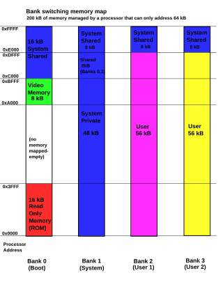
Bank switching is a technique used in computer design to increase the amount of usable memory beyond the amount directly addressable by the processor instructions. It can be used to configure a system differently at different times; for example, a ROM required to start a system from diskette could be switched out when no longer needed. In video game systems, bank switching allowed larger games to be developed for play on existing consoles.

<span class="mw-page-title-main">Zilog Z8000</span> 16-bit microprocessor

The Z8000 is a 16-bit microprocessor introduced by Zilog in early 1979. The architecture was designed by Bernard Peuto while the logic and physical implementation was done by Masatoshi Shima, assisted by a small group of people. In contrast to most designs of the era, the Z8000 did not use microcode which allowed it to be implemented in only 17,500 transistors.

In computing, Physical Address Extension (PAE), sometimes referred to as Page Address Extension, is a memory management feature for the x86 architecture. PAE was first introduced by Intel in the Pentium Pro, and later by AMD in the Athlon processor. It defines a page table hierarchy of three levels (instead of two), with table entries of 64 bits each instead of 32, allowing these CPUs to directly access a physical address space larger than 4 gigabytes (232 bytes).

<span class="mw-page-title-main">Extended memory</span>

In DOS memory management, extended memory refers to memory above the first megabyte (220 bytes) of address space in an IBM PC or compatible with an 80286 or later processor. The term is mainly used under the DOS and Windows operating systems. DOS programs, running in real mode or virtual x86 mode, cannot directly access this memory, but are able to do so through an application programming interface called the Extended Memory Specification (XMS). This API is implemented by a driver (such as HIMEM.SYS) or the operating system, which takes care of memory management and copying memory between conventional and extended memory, by temporarily switching the processor into protected mode. In this context, the term "extended memory" may refer to either the whole of the extended memory or only the portion available through this API.

<span class="mw-page-title-main">Expanded memory</span> System of bank switching in DOS memory management

In DOS memory management, expanded memory is a system of bank switching that provided additional memory to DOS programs beyond the limit of conventional memory (640 KiB).

<span class="mw-page-title-main">Conventional memory</span> First 640K of RAM under DOS

In DOS memory management, conventional memory, also called base memory, is the first 640 kilobytes of the memory on IBM PC or compatible systems. It is the read-write memory directly addressable by the processor for use by the operating system and application programs. As memory prices rapidly declined, this design decision became a limitation in the use of large memory capacities until the introduction of operating systems and processors that made it irrelevant.

<span class="mw-page-title-main">Memory address</span> Reference to a specific memory location

In computing, a memory address is a reference to a specific memory location used at various levels by software and hardware. Memory addresses are fixed-length sequences of digits conventionally displayed and manipulated as unsigned integers. Such numerical semantic bases itself upon features of CPU, as well upon use of the memory like an array endorsed by various programming languages.

In computing, the term 3 GB barrier refers to a limitation of some 32-bit operating systems running on x86 microprocessors. It prevents the operating systems from using all of 4 GiB (4 × 10243 bytes) of main memory. The exact barrier varies by motherboard and I/O device configuration, particularly the size of video RAM; it may be in the range of 2.75 GB to 3.5 GB. The barrier is not present with a 64-bit processor and 64-bit operating system, or with certain x86 hardware and an operating system such as Linux or certain versions of Windows Server and macOS that allow use of Physical Address Extension (PAE) mode on x86 to access more than 4 GiB of RAM.

References

  1. "AMD64 Programmer's Manual Volume 2: System Programming" (PDF). Advanced Micro Devices. December 2016. p. 120.
  2. "Intel 64 and IA-32 Architectures Software Developer's Manual Volume 3A: System Programming Guide, Part 1" (PDF). Intel. September 2016. p. 4-2.
  3. "ARM Architecture Reference Manual ARMv8, for ARMv8-A architecture profile". pp. D4-1723, D4-1724, D4-1731.
  4. http://infocenter.arm.com/help/topic/com.arm.doc.den0001c/DEN0001C_principles_of_arm_memory_maps.pdf [ bare URL PDF ]