
A multivibrator is an electronic circuit used to implement a variety of simple two-state devices such as relaxation oscillators, timers and flip-flops. It consists of two amplifying devices cross-coupled by resistors or capacitors. The first multivibrator circuit, the astable multivibrator oscillator, was invented by Henri Abraham and Eugene Bloch during World War I. They called their circuit a "multivibrator " because its output waveform was rich in harmonics.

The metal–oxide–semiconductor field-effect transistor, also known as the metal–oxide–silicon transistor, is a type of insulated-gate field-effect transistor that is fabricated by the controlled oxidation of a semiconductor, typically silicon. The voltage of the covered gate determines the electrical conductivity of the device; this ability to change conductivity with the amount of applied voltage can be used for amplifying or switching electronic signals.
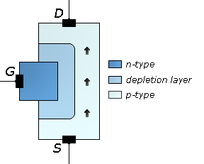
The junction-gate field-effect transistor (JFET) is one of the simplest types of field-effect transistor. JFETs are three-terminal semiconductor devices that can be used as electronically controlled switches or resistors, or to build amplifiers.

A bipolar junction transistor (BJT) is a type of transistor that uses both electrons and electron holes as charge carriers. In contrast, a unipolar transistor, such as a field-effect transistor, uses only one kind of charge carrier. A bipolar transistor allows a small current injected at one of its terminals to control a much larger current flowing between two other terminals, making the device capable of amplification or switching.

The 555 timer IC is an integrated circuit (chip) used in a variety of timer, delay, pulse generation, and oscillator applications. Derivatives provide two (556) or four (558) timing circuits in one package. It was commercialized in 1972 by Signetics. Numerous companies have made the original bipolar timers and similar low-power CMOS timers too. In 2017, it was said over a billion 555 timers are produced annually by some estimates, and "probably the most popular integrated circuit ever made."
Brokaw bandgap reference is a voltage reference circuit widely used in integrated circuits, with an output voltage around 1.25 V with low temperature dependence. This particular circuit is one type of a bandgap voltage reference, named after Paul Brokaw, the author of its first publication.
A bandgap voltage reference is a temperature independent voltage reference circuit widely used in integrated circuits. It produces a fixed (constant) voltage regardless of power supply variations, temperature changes, or circuit loading from a device. It commonly has an output voltage around 1.25 V. This circuit concept was first published by David Hilbiber in 1964. Bob Widlar, Paul Brokaw and others followed up with other commercially successful versions.
A current mirror is a circuit designed to copy a current through one active device by controlling the current in another active device of a circuit, keeping the output current constant regardless of loading. The current being "copied" can be, and sometimes is, a varying signal current. Conceptually, an ideal current mirror is simply an ideal inverting current amplifier that reverses the current direction as well. Or it can consist of a current-controlled current source (CCCS). The current mirror is used to provide bias currents and active loads to circuits. It can also be used to model a more realistic current source.

A p–n junction is a boundary or interface between two types of semiconductor materials, p-type and n-type, inside a single crystal of semiconductor. The "p" (positive) side contains an excess of holes, while the "n" (negative) side contains an excess of electrons in the outer shells of the electrically neutral atoms there. This allows electrical current to pass through the junction only in one direction. The p-n junction is created by doping, for example by ion implantation, diffusion of dopants, or by epitaxy. If two separate pieces of material were used, this would introduce a grain boundary between the semiconductors that would severely inhibit its utility by scattering the electrons and holes.

A current source is an electronic circuit that delivers or absorbs an electric current which is independent of the voltage across it.
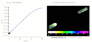
The threshold voltage, commonly abbreviated as Vth, of a field-effect transistor (FET) is the minimum gate-to-source voltage VGS (th) that is needed to create a conducting path between the source and drain terminals. It is an important scaling factor to maintain power efficiency.
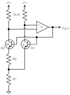
A Widlar current source is a modification of the basic two-transistor current mirror that incorporates an emitter degeneration resistor for only the output transistor, enabling the current source to generate low currents using only moderate resistor values.
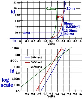
In electronics, diode modelling refers to the mathematical models used to approximate the actual behaviour of real diodes to enable calculations and circuit analysis. A diode's I-V curve is nonlinear.
The Shockley diode equation or the diode law, named after transistor co-inventor William Shockley of Bell Telephone Laboratories, gives the I–V (current-voltage) characteristic of an idealized diode in either forward or reverse bias :
A definition in semiconductor physics, carrier lifetime is defined as the average time it takes for a minority carrier to recombine. The process through which this is done is typically known as minority carrier recombination.

Bipolar transistors must be properly biased to operate correctly. In circuits made with individual devices, biasing networks consisting of resistors are commonly employed. Much more elaborate biasing arrangements are used in integrated circuits, for example, bandgap voltage references and current mirrors. The voltage divider configuration achieves the correct voltages by the use of resistors in certain patterns. By selecting the proper resistor values, stable current levels can be achieved that vary only little over temperature and with transistor properties such as β.
A log amplifier is an amplifier for which the output voltage Vout is K times the natural log of the input voltage Vin. This can be expressed as,

Multi-junction (MJ) solar cells are solar cells with multiple p–n junctions made of different semiconductor materials. Each material's p-n junction will produce electric current in response to different wavelengths of light. The use of multiple semiconducting materials allows the absorbance of a broader range of wavelengths, improving the cell's sunlight to electrical energy conversion efficiency.

In physics, the Shockley–Queisser limit is the maximum theoretical efficiency of a solar cell using a single p-n junction to collect power from the cell where the only loss mechanism is radiative recombination in the solar cell. It was first calculated by William Shockley and Hans-Joachim Queisser at Shockley Semiconductor in 1961, giving a maximum efficiency of 30% at 1.1 eV. This first calculation used the 6000K black-body spectrum as an approximation to the solar spectrum. Subsequent calculations have used measured global solar spectra (AM1.5G) and included a back surface mirror which increases the maximum efficiency to 33.7% for a solar cell with a bandgap of 1.34 eV. The limit is one of the most fundamental to solar energy production with photovoltaic cells, and is considered to be one of the most important contributions in the field.

The theory of solar cells explains the process by which light energy in photons is converted into electric current when the photons strike a suitable semiconductor device. The theoretical studies are of practical use because they predict the fundamental limits of a solar cell, and give guidance on the phenomena that contribute to losses and solar cell efficiency.


