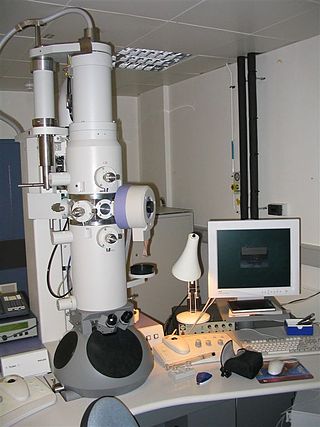
An electron microscope is a microscope that uses a beam of electrons as a source of illumination. They use electron optics that are analogous to the glass lenses of an optical light microscope to control the electron beam, for instance focusing them to produce magnified images or electron diffraction patterns. As the wavelength of an electron can be up to 100,000 times smaller than that of visible light, electron microscopes have a much higher resolution of about 0.1 nm, which compares to about 200 nm for light microscopes. Electron microscope may refer to:

A microscope is a laboratory instrument used to examine objects that are too small to be seen by the naked eye. Microscopy is the science of investigating small objects and structures using a microscope. Microscopic means being invisible to the eye unless aided by a microscope.

A scanning electron microscope (SEM) is a type of electron microscope that produces images of a sample by scanning the surface with a focused beam of electrons. The electrons interact with atoms in the sample, producing various signals that contain information about the surface topography and composition of the sample. The electron beam is scanned in a raster scan pattern, and the position of the beam is combined with the intensity of the detected signal to produce an image. In the most common SEM mode, secondary electrons emitted by atoms excited by the electron beam are detected using a secondary electron detector. The number of secondary electrons that can be detected, and thus the signal intensity, depends, among other things, on specimen topography. Some SEMs can achieve resolutions better than 1 nanometer.

Thomas Eugene Everhart FREng is an American educator and physicist. His area of expertise is the physics of electron beams. Together with Richard F. M. Thornley he designed the Everhart–Thornley detector. These detectors are still in use in scanning electron microscopes, even though the first such detector was made available as early as 1956.
A microprobe is an instrument that applies a stable and well-focused beam of charged particles to a sample.

Alec Nigel Broers, Baron Broers, is a British electrical engineer.

The Department of Materials at the University of Oxford, England was founded in the 1950s as the Department of Metallurgy, by William Hume-Rothery, who was a reader in Oxford's Department of Inorganic Chemistry. It is part of the university's Mathematical, Physical and Life Sciences Division
Failure analysis is the process of collecting and analyzing data to determine the cause of a failure, often with the goal of determining corrective actions or liability. According to Bloch and Geitner, ”machinery failures reveal a reaction chain of cause and effect… usually a deficiency commonly referred to as the symptom…”. Failure analysis can save money, lives, and resources if done correctly and acted upon. It is an important discipline in many branches of manufacturing industry, such as the electronics industry, where it is a vital tool used in the development of new products and for the improvement of existing products. The failure analysis process relies on collecting failed components for subsequent examination of the cause or causes of failure using a wide array of methods, especially microscopy and spectroscopy. Nondestructive testing (NDT) methods are valuable because the failed products are unaffected by analysis, so inspection sometimes starts using these methods.

Focused ion beam, also known as FIB, is a technique used particularly in the semiconductor industry, materials science and increasingly in the biological field for site-specific analysis, deposition, and ablation of materials. A FIB setup is a scientific instrument that resembles a scanning electron microscope (SEM). However, while the SEM uses a focused beam of electrons to image the sample in the chamber, a FIB setup uses a focused beam of ions instead. FIB can also be incorporated in a system with both electron and ion beam columns, allowing the same feature to be investigated using either of the beams. FIB should not be confused with using a beam of focused ions for direct write lithography. These are generally quite different systems where the material is modified by other mechanisms.

A scanning helium ion microscope is an imaging technology based on a scanning helium ion beam. Similar to other focused ion beam techniques, it allows to combine milling and cutting of samples with their observation at sub-nanometer resolution.
Electron-beam-induced deposition (EBID) is a process of decomposing gaseous molecules by an electron beam leading to deposition of non-volatile fragments onto a nearby substrate. The electron beam is usually provided by a scanning electron microscope, which results in high spatial accuracy and the possibility to produce free-standing, three-dimensional structures.

FEI Company was an American company that designed, manufactured, and supported microscope technology. Headquartered in Hillsboro, Oregon, FEI had over 2,800 employees and sales and service operations in more than 50 countries around the world. Formerly listed on the NASDAQ, it is now a subsidiary of Thermo Fisher Scientific.

Rigaku Corporation is an international manufacturer and distributor of scientific, analytical and industrial instrumentation specializing in X-ray related technologies, including X-ray crystallography, X-ray diffraction (XRD), X-ray reflectivity, X-ray fluorescence (XRF), automation, cryogenics and X-ray optics.
Serial block-face scanning electron microscopy is a method to generate high resolution three-dimensional images from small samples. The technique was developed for brain tissue, but it is widely applicable for any biological samples. A serial block-face scanning electron microscope consists of an ultramicrotome mounted inside the vacuum chamber of a scanning electron microscope. Samples are prepared by methods similar to that in transmission electron microscopy (TEM), typically by fixing the sample with aldehyde, staining with heavy metals such as osmium and uranium then embedding in an epoxy resin. The surface of the block of resin-embedded sample is imaged by detection of back-scattered electrons. Following imaging the ultramicrotome is used to cut a thin section from the face of the block. After the section is cut, the sample block is raised back to the focal plane and imaged again. This sequence of sample imaging, section cutting and block raising can acquire many thousands of images in perfect alignment in an automated fashion. Practical serial block-face scanning electron microscopy was invented in 2004 by Winfried Denk at the Max-Planck-Institute in Heidelberg and is commercially available from Gatan Inc., Thermo Fisher Scientific (VolumeScope) and ConnectomX.

Mountains is an image analysis and surface metrology software platform published by the company Digital Surf. Its core is micro-topography, the science of studying surface texture and form in 3D at the microscopic scale. The software is dedicated to profilometers, 3D light microscopes ("MountainsMap"), scanning electron microscopes ("MountainsSEM") and scanning probe microscopes ("MountainsSPIP").
Soquelec limited is a Montreal-based company that focuses on sales and service of scientific equipment for applications in materials and life sciences. It is the Canadian distributor of manufacturers of digital imaging technology and accessories, such as Electron Microscopy, Atomic Force Microscopy, X-Ray scanning and sample preparation. It is also a provider of laboratory consumables. Its sister company, Soquelec Telecommunications, specializes in the distribution of RF, microwave and millimeter-wave telecommunication components.
The Austrian Centre for Electron Microscopy and Nanoanalysis is a cooperation between the Institute of Electron Microscopy and Nanoanalysis (FELMI) of the Graz University of Technology (TUG) and the Graz Centre of Electron Microscopy (ZFE), which is a member of Austrian Cooperative Research (ACR) and run by the non-profit association for the promotion of electron microscopy. It is located at the “Neue Technik Steyrergasse” campus in Graz.

Transmission Kikuchi Diffraction (TKD), also sometimes called transmission-electron backscatter diffraction (t-EBSD), is a method for orientation mapping at the nanoscale. It’s used for analysing the microstructures of thin transmission electron microscopy (TEM) specimens in the scanning electron microscope (SEM). This technique has been widely utilised in the characterization of nano-crystalline materials, including oxides, superconductors, and metallic alloys.
Teodor Paweł Gotszalk is a Polish scientist who is head of Department of Nanometrology at Wrocław University of Science and Technology. Corresponding member of Polish Academy of Sciences since 2022. Teodor Gotszalk works in the area of nanotechnology and nanometrology, particularly scanning probe microscopy (SPM), scanning electron microscopy (SEM) and focused ion beam (FIB) techniques, and using microelectromechanical systems (MEMS).
