Precession electron diffraction

Last updated
Geometry of electron beam in precession electron diffraction. Original diffraction patterns collected by C.S. Own at Northwestern University Precession Electron Diffraction (White).gif
Geometry of electron beam in precession electron diffraction. Original diffraction patterns collected by C.S. Own at Northwestern University

Precession electron diffraction (PED) is a specialized method to collect electron diffraction patterns in a transmission electron microscope (TEM). By rotating (precessing) a tilted incident electron beam around the central axis of the microscope, a PED pattern is formed by integration over a collection of diffraction conditions. This produces a quasi-kinematical diffraction pattern that is more suitable as input into direct methods algorithms to determine the crystal structure of the sample.

Contents

Overview

Geometry

Precession electron diffraction is accomplished utilizing the standard instrument configuration of a modern TEM. The animation illustrates the geometry used to generate a PED pattern. Specifically, the beam tilt coils located pre-specimen are used to tilt the electron beam off of the optic axis so it is incident with the specimen at an angle, φ. The image shift coils post-specimen are then used to tilt the diffracted beams back in a complementary manner such that the direct beam falls in the center of the diffraction pattern. Finally, the beam is precessed around the optic axis while the diffraction pattern is collected over multiple revolutions.

The result of this process is a diffraction pattern that consists of a summation or integration over the patterns generated during precession. While the geometry of this pattern matches the pattern associated with a normally incident beam, the intensities of the various reflections approximate those of the kinematical pattern much more closely. At any moment in time during precession, the diffraction pattern consists of a Laue circle with a radius equal to the precession angle, φ. It is crucial to note that these snapshots contain far fewer strongly excited reflections than a normal zone axis pattern and extend farther into reciprocal space. Thus, the composite pattern will display far less dynamical character, and will be well suited for use as input into direct methods calculations. [2]

Advantages

PED possesses many advantageous attributes that make it well suited to investigating crystal structures via direct methods approaches: [1]

  1. Quasi-kinematical diffraction patterns: While the underlying physics of the electron diffraction is still dynamical in nature, the conditions used to collect PED patterns minimize many of these effects. The scan/de-scan procedure reduces ion channeling because the pattern is generated off of the zone axis. Integration via precession of the beam minimizes the effect of non-systematic inelastic scattering, such as Kikuchi lines. Few reflections are strongly excited at any moment during precession, and those that are excited are generally much closer to a two-beam condition (dynamically coupled only to the forward-scattered beam). Furthermore, for large precession angles, the radius of the excited Laue circle becomes quite large. These contributions combine such that the overall integrated diffraction pattern resembles the kinematical pattern much more closely than a single zone axis pattern.
  2. Broader range of measured reflections: The Laue circle (see Ewald sphere) that is excited at any given moment during precession extends farther into reciprocal space. After integration over multiple precessions, many more reflections in the zeroeth order Laue zone (ZOLZ) are present, and as stated previously, their relative intensities are much more kinematical. This provides considerably more information to input into direct methods calculations, improving the accuracy of phase determination algorithms. Similarly, more higher order Laue zone (HOLZ) reflections are present in the pattern, which can provide more complete information about the three-dimensional nature of reciprocal space, even in a single two-dimensional PED pattern.
  3. Practical robustness: PED is less sensitive to small experimental variations than other electron diffraction techniques. Since the measurement is an average over many incident beam directions, the pattern is less sensitive to slight misorientation of the zone axis from the optic axis of the microscope, and resulting PED patterns will generally still display the zone axis symmetry. The patterns obtained are also less sensitive to the thickness of the sample, a parameter with strong influence in standard electron diffraction patterns.
  4. Very small probe size: Because x-rays interact so weakly with matter, there is a minimum size limit of approximately 5 µm for single crystals that can be examined via x-ray diffraction methods. In contrast, electrons can be used to probe much smaller nano-crystals in a TEM. In PED, the probe size is limited by the lens aberrations and sample thickness. With a typical value for spherical aberration, the minimum probe size is usually around 50 nm. However, with Cs corrected microscopes, the probe can be made much smaller.

Practical considerations

Precession electron diffraction is typically conducted using accelerating voltages between 100-400 kV. Patterns can be formed under parallel or convergent beam conditions. Most modern TEMs can achieve a tilt angle, φ, ranging from 0-3°. Precession frequencies can be varied from Hz to kHz, but in standard cases 60 Hz has been used. [1] In choosing a precession rate, it is important to ensure that many revolutions of the beam occur over the relevant exposure time used to record the diffraction pattern. This ensures adequate averaging over the excitation error of each reflection. Beam sensitive samples may dictate shorter exposure times and thus, motivate the use of higher precession frequencies.

One of the most significant parameters affecting the diffraction pattern obtained is the precession angle, φ. In general, larger precession angles result in more kinematical diffraction patterns, but both the capabilities of the beam tilt coils in the microscope and the requirements on the probe size limit how large this angle can become in practice. Because PED takes the beam off of the optic axis by design, it accentuates the effect of the spherical aberrations within the probe forming lens. For a given spherical aberration, Cs, the probe diameter, d, varies with convergence angle, α, and precession angle, φ, as [3]

Thus, if the specimen of interest is quite small, the maximum precession angle will be restrained. This is most significant for conditions of convergent beam illumination. 50 nm is a general lower limit on probe size for standard TEMs operating at high precession angles (>30  mrad), but can be surpassed in Cs corrected instruments. [4] In principle the minimum precessed probe can reach approximately the full-width-half-max (FWHM) of the converged un-precessed probe in any instrument, however in practice the effective precessed probe is typically ~10-50x larger due to uncontrolled aberrations present at high angles of tilt. For example, a 2 nm precessed probe with >40 mrad precession angle was demonstrated in an aberration-corrected Nion UltraSTEM with native sub-Å probe (aberrations corrected to ~35 mrad half-angle). [5]

If the precession angle is made too large, further complications due to the overlap of the ZOLZ and HOLZ reflections in the projected pattern can occur. This complicates the indexing of the diffraction pattern and can corrupt the measured intensities of reflections near the overlap region, thereby reducing the effectiveness of the collected pattern for direct methods calculations.

Theoretical considerations

For an introduction to the theory of electron diffraction, see part 2 of Williams and Carter's Transmission Electron Microscopy text [6]

While it is clear that precession reduces many of the dynamical diffraction effects that plague other forms of electron diffraction, the resulting patterns cannot be considered purely kinematical in general. There are models that attempt to introduce corrections to convert measured PED patterns into true kinematical patterns that can be used for more accurate direct methods calculations, with varying degrees of success. Here, the most basic corrections are discussed. In purely kinematical diffraction, the intensities of various reflections, , are related to the square of the amplitude of the structure factor, by the equation:

This relationship is generally far from accurate for experimental dynamical electron diffraction and when many reflections have a large excitation error. First, a Lorentz correction analogous to that used in x-ray diffraction can be applied to account for the fact that reflections are infrequently exactly at the Bragg condition over the course of a PED measurement. This geometrical correction factor can be shown to assume the approximate form: [7]

where g is the reciprocal space magnitude of the reflection in question and Ro is the radius of the Laue circle, usually taken to be equal to φ. While this correction accounts for the integration over the excitation error, it takes no account for the dynamical effects that are ever-present in electron diffraction. This has been accounted for using a two-beam correction following the form of the Blackman correction originally developed for powder x-ray diffraction. Combining this with the aforementioned Lorentz correction yields:

where , is the sample thickness, and is the wave-vector of the electron beam. is the Bessel function of zeroeth order.

This form seeks to correct for both geometric and dynamical effects, but is still only an approximation that often fails to significantly improve the kinematic quality of the diffraction pattern (sometimes even worsening it). More complete and accurate treatments of these theoretical correction factors have been shown to adjust measured intensities into better agreement with kinematical patterns. For details, see Chapter 4 of reference. [1]

Only by considering the full dynamical model through multislice calculations can the diffraction patterns generated by PED be simulated. However, this requires the crystal potential to be known, and thus is most valuable in refining the crystal potentials suggested through direct methods approaches. The theory of precession electron diffraction is still an active area of research, and efforts to improve on the ability to correct measured intensities without a priori knowledge are ongoing.

Historical development

The first precession electron diffraction system was developed by Vincent and Midgley in Bristol, UK and published in 1994. Preliminary investigation into the Er2Ge2O7 crystal structure demonstrated the feasibility of the technique at reducing dynamical effects and providing quasi-kinematical patterns that could be solved through direct methods to determine crystal structure. [3] Over the next ten years, a number of university groups developed their own precession systems and verified the technique by solving complex crystal structures, including the groups of J. Gjønnes (Oslo), Migliori (Bologna), and L. Marks (Northwestern). [1] [8] [9] [10] [11]

In 2004, NanoMEGAS developed the first commercial precession system capable of being retrofit to any modern TEM. This hardware solution enabled more widespread implementation of the technique and spurred its more mainstream adoption into the crystallography community. Software methods have also been developed to achieve the necessary scanning and descanning using the built-in electronics of the TEM. [12] HREM Research Inc has developed the QED plug-in for the DigitalMicrograph software. This plug-in enables the widely used software package to collect precession electron diffraction patterns without additional modifications to the microscope.

According to NanoMEGAS, as of June, 2015, more than 200 publications have relied on the technique to solve or corroborate crystal structures; many on materials that could not be solved by other conventional crystallography techniques like x-ray diffraction. Their retrofit hardware system is used in more than 75 laboratories across the world. [13]

Applications

Crystallography

The primary goal of crystallography is to determine the three dimensional arrangement of atoms in a crystalline material. While historically, x-ray crystallography has been the predominant experimental method used to solve crystal structures ab initio, the advantages of precession electron diffraction make it one of the preferred methods of electron crystallography.

Symmetry determination

The symmetry of a crystalline material has profound impacts on its emergent properties, including electronic band structure, electromagnetic behavior, and mechanical properties . Crystal symmetry is described and categorized by the crystal system, lattice, and space group of the material. Determination of these attributes is an important aspect of crystallography.
Precession electron diffraction enables much more direct determination of space group symmetries over other forms of electron diffraction. Because of the increased number of reflections in both the zero order Laue zone and higher order Laue zones, the geometric relationship between Laue zones is more readily determined. This provides three-dimensional information about the crystal structure that can be used to determine its space group. [14] [15] Furthermore, because the PED technique is insensitive to slight misorientation from the zone axis, it provides the practical benefit of more robust data collection. [16]

Direct methods

Direct methods in crystallography are a collection of mathematical techniques that seek to determine crystal structure based on measurements of diffraction patterns and potentially other a priori knowledge (constraints). The central challenge of inverting measured diffraction intensities (i.e. applying an inverse Fourier Transform) to determine the original crystal potential is that phase information is lost in general since intensity is a measurement of the square of the modulus of the amplitude of any given diffracted beam. This is known as the phase problem of crystallography.
If the diffraction can be considered kinematical, constraints may be used to probabilistically relate the phases of the reflections to their amplitudes, and the original structure can be solved via direct methods (see Sayre equation as an example). Kinematical diffraction is often the case in x-ray diffraction, and is one of the primary reasons that technique has been so successful at solving crystal structures. However, in electron diffraction, the probing wave interacts much more strongly with the electrostatic crystal potential, and complex dynamical diffraction effects can dominate the measured diffraction patterns. This makes application of direct methods much more challenging without a priori knowledge of the structure in question.

Ab Initio structure determination

Diffraction patterns collected through PED often agree well-enough with the kinematical pattern to serve as input data for direct methods calculations. A three-dimensional set of intensities mapped over the reciprocal lattice can be generated by collecting diffraction patterns over multiple zone axes. Applying direct methods to this data set will then yield probable crystal structures. Coupling direct methods results with simulations (e.g. multislice) and iteratively refining the solution can lead to the ab initio determination of the crystal structure. [16] [17]
The PED technique has been used to determine the crystal structure of many classes of materials. Initial investigations during the emergence of the technique focused on complex oxides [1] [18] and nano-precipitates in Aluminum alloys that could not be resolved using x-ray diffraction. [19] Since becoming a more widespread crystallographic technique, many more complex metal oxide structures have been solved. [20] [21] [22] [23]
Example of a zeolite structure Zeolite-ZSM-5-3D-vdW.png
Example of a zeolite structure
Zeolites are a technologically valuable class of materials that have historically been difficult to solve using x-ray diffraction due to the large unit cells that typically occur. PED has been demonstrated to be a viable alternative to solving many of these structures, including the ZSM-10, MCM-68, and many of the ITQ-n class of zeolite structures. [23] [24]
PED also enables the use of electron diffraction to investigate beam-sensitive organic materials. Because PED can reproduce symmetric zone axis diffraction patterns even when the zone axis is not perfectly aligned, it enables information to be extracted from sensitive samples without risking overexposure during a time-intensive orientation of the sample. [4]

Automated diffraction tomography

Automated diffraction tomography (ADT) uses software to collect diffraction patterns over a series of slight tilt increments. In this way, a three-dimensional (tomographic) data set of reciprocal lattice intensities can be generated and used for structure determination. By coupling this technique with PED, the range and quality of the data set can be improved. [25] The combination of ADT-PED has been employed effectively to investigate complex framework structures [26] [27] and beam-sensitive organic crystals [28]

Orientation mapping

ASTAR TEM Orientation imaging of gold particles, courtesy of Dr. Mauro Gemmi, IIT Pisa Italia TEM Orientation Mapping.png
ASTAR TEM Orientation imaging of gold particles, courtesy of Dr. Mauro Gemmi, IIT Pisa Italia

Mapping the relative orientation of crystalline grains and/or phases helps understand material texture at the micro and nano scales. In a transmission electron microscope, this is accomplished by recording a diffraction pattern at a large number of points (pixels) over a region of the crystalline specimen. By comparing the recorded patterns to a database of known patterns (either previously indexed experimental patterns or simulated patterns), the relative orientation of grains in the field of view can be determined.

Because this process is highly automated, the quality of the recorded diffraction patterns is crucial to the software's ability to accurately compare and assign orientations to each pixel. Thus, the advantages of PED are well-suited for use with this scanning technique. By instead recording a PED pattern at each pixel, dynamical effects are reduced, and the patterns are more easily compared to simulated data, improving the accuracy of the automated phase/orientation assignment. [4]

Beyond diffraction

Although the PED technique was initially developed for its improved diffraction applications, the advantageous properties of the technique have been found to enhance many other investigative techniques in the TEM. These include bright field and dark field imaging, electron tomography, and composition-probing techniques like energy-dispersive x-ray spectroscopy (EDS) and electron energy loss spectroscopy (EELS).

Imaging

Though many people conceptualize images and diffraction patterns separately, they contain principally the same information. In the simplest approximation, the two are simply Fourier transforms of one another. Thus, the effects of beam precession on diffraction patterns also have significant effects on the corresponding images in the TEM. Specifically, the reduced dynamical intensity transfer between beams that is associated with PED results in reduced dynamical contrast in images collected during precession of the beam. This includes a reduction in thickness fringes, bend contours, and strain fields. [13] While these features can often provide useful information, their suppression enables a more straightforward interpretation of diffraction contrast and mass contrast in images.

Tomography

In an extension of the application of PED to imaging, electron tomography can benefit from the reduction of dynamic contrast effects. Tomography entails collecting a series of images (2-D projections) at various tilt angles and combining them to reconstruct the three dimensional structure of the specimen. Because many dynamical contrast effects are highly sensitive to the orientation of the crystalline sample with respect to the incident beam, these effects can convolute the reconstruction process in tomography. Similarly to single imaging applications, by reducing dynamical contrast, interpretation of the 2-D projections and thus the 3-D reconstruction are more straightforward.

Investigating composition

Energy-dispersive x-ray spectroscopy (EDS) and electron energy loss spectroscopy (EELS) are commonly used techniques to both qualitatively and quantitatively probe the composition of samples in the TEM. A primary challenge in the quantitative accuracy of both techniques is the phenomenon of channelling. Put simply, in a crystalline solid, the probability of interaction between an electron and ion in the lattice depends strongly on the momentum (direction and velocity) of the electron. When probing a sample under diffraction conditions near a zone axis, as is often the case in EDS and EELS applications, channelling can have a large impact on the effective interaction of the incident electrons with specific ions in the crystal structure. In practice, this can lead to erroneous measurements of composition that depend strongly on the orientation and thickness of the sample and the accelerating voltage. Since PED entails an integration over incident directions of the electron probe, and generally does not include beams parallel to the zone axis, the detrimental channeling effects outlined above can be minimized, yielding far more accurate composition measurements in both techniques. [29] [30]

Related Research Articles

<span class="mw-page-title-main">X-ray crystallography</span> Technique used for determining crystal structures and identifying mineral compounds

X-ray crystallography is the experimental science determining the atomic and molecular structure of a crystal, in which the crystalline structure causes a beam of incident X-rays to diffract into many specific directions. By measuring the angles and intensities of these diffracted beams, a crystallographer can produce a three-dimensional picture of the density of electrons within the crystal. From this electron density, the mean positions of the atoms in the crystal can be determined, as well as their chemical bonds, their crystallographic disorder, and various other information.

<span class="mw-page-title-main">Transmission electron microscopy</span> Imaging and diffraction using electrons that pass through samples

Transmission electron microscopy (TEM) is a microscopy technique in which a beam of electrons is transmitted through a specimen to form an image. The specimen is most often an ultrathin section less than 100 nm thick or a suspension on a grid. An image is formed from the interaction of the electrons with the sample as the beam is transmitted through the specimen. The image is then magnified and focused onto an imaging device, such as a fluorescent screen, a layer of photographic film, or a sensor such as a scintillator attached to a charge-coupled device.

<span class="mw-page-title-main">Electron diffraction</span> Bending of electron beams due to electrostatic interactions with matter

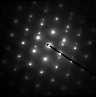
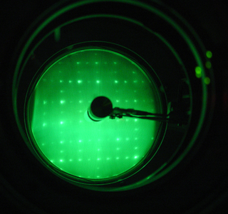
Electron diffraction is a general term for phenomena associated with changes in the direction of electron beams due to elastic interactions with atoms. Close to the atoms the changes are described as Fresnel diffraction; far away they are called Fraunhofer diffraction. The resulting map of the directions of the electrons far from the sample is called a diffraction pattern, see for instance Figure 1. These patterns are similar to x-ray and neutron diffraction patterns, and are used to study the atomic structure of gases, liquids, surfaces and bulk solids. Electron diffraction also plays a major role in the contrast of images in electron microscopes.

Reflection high-energy electron diffraction (RHEED) is a technique used to characterize the surface of crystalline materials. RHEED systems gather information only from the surface layer of the sample, which distinguishes RHEED from other materials characterization methods that also rely on diffraction of high-energy electrons. Transmission electron microscopy, another common electron diffraction method samples mainly the bulk of the sample due to the geometry of the system, although in special cases it can provide surface information. Low-energy electron diffraction (LEED) is also surface sensitive, but LEED achieves surface sensitivity through the use of low energy electrons.

<span class="mw-page-title-main">Neutron scattering</span> Physical phenomenon

Neutron scattering, the irregular dispersal of free neutrons by matter, can refer to either the naturally occurring physical process itself or to the man-made experimental techniques that use the natural process for investigating materials. The natural/physical phenomenon is of elemental importance in nuclear engineering and the nuclear sciences. Regarding the experimental technique, understanding and manipulating neutron scattering is fundamental to the applications used in crystallography, physics, physical chemistry, biophysics, and materials research.

The Ewald sphere is a geometric construction used in electron, neutron, and x-ray diffraction which shows the relationship between:

<span class="mw-page-title-main">Electron backscatter diffraction</span> Scanning electron microscopy technique

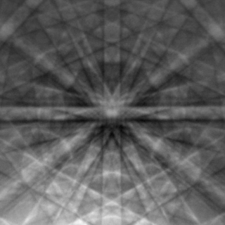
Electron backscatter diffraction (EBSD) is a scanning electron microscopy (SEM) technique used to study the crystallographic structure of materials. EBSD is carried out in a scanning electron microscope equipped with an EBSD detector comprising at least a phosphorescent screen, a compact lens and a low-light camera. In this configuration, the SEM incident beam hits the tilted sample. As backscattered electrons leave the sample, they interact with the crystal's periodic atomic lattice planes and diffract according to Bragg's law at various scattering angles before reaching the phosphor screen forming Kikuchi patterns (EBSPs). EBSD spatial resolution depends on many factors, including the nature of the material under study and the sample preparation. Thus, EBSPs can be indexed to provide information about the material's grain structure, grain orientation, and phase at the micro-scale. EBSD is applied for impurities and defect studies, plastic deformation, and statistical analysis for average misorientation, grain size, and crystallographic texture. EBSD can also be combined with energy-dispersive X-ray spectroscopy (EDS), cathodoluminescence (CL), and wavelength-dispersive X-ray spectroscopy (WDS) for advanced phase identification and materials discovery.

Electron crystallography is a method to determine the arrangement of atoms in solids using a transmission electron microscope (TEM). It can involve the use of high-resolution transmission electron microscopy images, electron diffraction patterns including convergent-beam electron diffraction or combinations of these. It has been successful in determining some bulk structures, and also surface structures. Two related methods are low-energy electron diffraction which has solved the structure of many surfaces, and reflection high-energy electron diffraction which is used to monitor surfaces often during growth.

<span class="mw-page-title-main">Scanning transmission electron microscopy</span> Scanning microscopy using thin samples and transmitted electrons

A scanning transmission electron microscope (STEM) is a type of transmission electron microscope (TEM). Pronunciation is [stɛm] or [ɛsti:i:ɛm]. As with a conventional transmission electron microscope (CTEM), images are formed by electrons passing through a sufficiently thin specimen. However, unlike CTEM, in STEM the electron beam is focused to a fine spot which is then scanned over the sample in a raster illumination system constructed so that the sample is illuminated at each point with the beam parallel to the optical axis. The rastering of the beam across the sample makes STEM suitable for analytical techniques such as Z-contrast annular dark-field imaging, and spectroscopic mapping by energy dispersive X-ray (EDX) spectroscopy, or electron energy loss spectroscopy (EELS). These signals can be obtained simultaneously, allowing direct correlation of images and spectroscopic data.

<span class="mw-page-title-main">Powder diffraction</span>

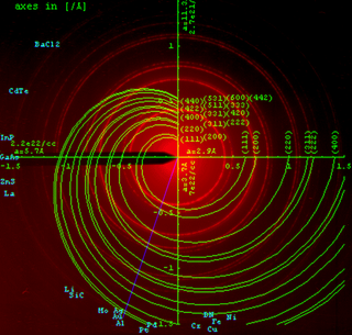
Powder diffraction is a scientific technique using X-ray, neutron, or electron diffraction on powder or microcrystalline samples for structural characterization of materials. An instrument dedicated to performing such powder measurements is called a powder diffractometer.

Phase-contrast imaging is a method of imaging that has a range of different applications. It measures differences in the refractive index of different materials to differentiate between structures under analysis. In conventional light microscopy, phase contrast can be employed to distinguish between structures of similar transparency, and to examine crystals on the basis of their double refraction. This has uses in biological, medical and geological science. In X-ray tomography, the same physical principles can be used to increase image contrast by highlighting small details of differing refractive index within structures that are otherwise uniform. In transmission electron microscopy (TEM), phase contrast enables very high resolution (HR) imaging, making it possible to distinguish features a few Angstrom apart.

<span class="mw-page-title-main">Selected area diffraction</span>

Selected area (electron) diffraction is a crystallographic experimental technique typically performed using a transmission electron microscope (TEM). It is a specific case of electron diffraction used primarily in material science and solid state physics as one of the most common experimental techniques. Especially with appropriate analytical software, SAD patterns (SADP) can be used to determine crystal orientation, measure lattice constants or examine its defects.

<span class="mw-page-title-main">Dynamical theory of diffraction</span>

The dynamical theory of diffraction describes the interaction of waves with a regular lattice. The wave fields traditionally described are X-rays, neutrons or electrons and the regular lattice are atomic crystal structures or nanometer-scale multi-layers or self-arranged systems. In a wider sense, similar treatment is related to the interaction of light with optical band-gap materials or related wave problems in acoustics. The sections below deal with dynamical diffraction of X-rays.

<span class="mw-page-title-main">Low-energy electron diffraction</span> Technique for determining surface structures

Low-energy electron diffraction (LEED) is a technique for the determination of the surface structure of single-crystalline materials by bombardment with a collimated beam of low-energy electrons (30–200 eV) and observation of diffracted electrons as spots on a fluorescent screen.

Helium atom scattering (HAS) is a surface analysis technique used in materials science. It provides information about the surface structure and lattice dynamics of a material by measuring the diffracted atoms from a monochromatic helium beam incident on the sample.

A crystallographic database is a database specifically designed to store information about the structure of molecules and crystals. Crystals are solids having, in all three dimensions of space, a regularly repeating arrangement of atoms, ions, or molecules. They are characterized by symmetry, morphology, and directionally dependent physical properties. A crystal structure describes the arrangement of atoms, ions, or molecules in a crystal.

Electron channelling contrast imaging (ECCI) is a scanning electron microscope (SEM) diffraction technique used in the study of defects in materials. These can be dislocations or stacking faults that are close to the surface of the sample, low angle grain boundaries or atomic steps. Unlike the use of transmission electron microscopy (TEM) for the investigation of dislocations, the ECCI approach has been called a rapid and non-destructive characterisation technique

<span class="mw-page-title-main">Convergent beam electron diffraction</span> Convergent beam electron diffraction technique

Convergent beam electron diffraction (CBED) is an electron diffraction technique where a convergent or divergent beam of electrons is used to study materials.

4D scanning transmission electron microscopy is a subset of scanning transmission electron microscopy (STEM) which utilizes a pixelated electron detector to capture a convergent beam electron diffraction (CBED) pattern at each scan location. This technique captures a 2 dimensional reciprocal space image associated with each scan point as the beam rasters across a 2 dimensional region in real space, hence the name 4D STEM. Its development was enabled by evolution in STEM detectors and improvements computational power. The technique has applications in visual diffraction imaging, phase orientation and strain mapping, phase contrast analysis, among others.

<span class="mw-page-title-main">Weak-beam dark-field microscopy</span> Electron microscopy technique

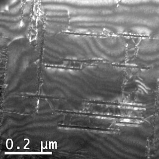
Weak beam dark field (WBDF) microscopy is a type of transmission electron microscopy (TEM) dark field imaging technique that allows for the visualization of crystal defects with high resolution and contrast. Specifically, the technique is mainly used to study crystal defects such as dislocations, stacking faults, and interfaces in crystalline materials. WBDF is a valuable tool for studying the microstructure of materials, as it can provide detailed information about the nature and distribution of defects in crystals. These characteristics can have a significant impact on material properties such as strength, ductility, and corrosion resistance.

References

  1. 1 2 3 4 5 6 Own, C. S.: PhD thesis, System Design and Verification of the Precession Electron Diffraction Technique, Northwestern University, 2005,http://www.numis.northwestern.edu/Research/Current/precession.shtml
  2. Notes from Advanced Electron Microscopy course at Northwestern University. Prepared by Professor Laurie Marks.
  3. 1 2 Vincent, R.; Midgley, P.A. (1994). "Double conical beam-rocking system for measurement of integrated electron diffraction intensities". Ultramicroscopy. 53 (3): 271–82. doi:10.1016/0304-3991(94)90039-6.
  4. 1 2 3 Eggeman, Alexander S.; Midgley, Paul A. (2012). "Precession Electron Diffraction". In Hawkes, Peter W. (ed.). Advances in Imaging and Electron Physics. Vol. 170. pp. 1–63. doi:10.1016/B978-0-12-394396-5.00001-4. ISBN   978-0-12-394396-5.
  5. Own, CS; Dellby, N; Krivanek, O; Marks, LD; Murfitt, M (2007). "Aberration-corrected Precession Electron Diffraction". Microscopy and Microanalysis. 13 (S02). doi:10.1017/S1431927607078555. S2CID   27057286.
  6. Williams, D.B.; Carter, C.B. (1996). Transmission Electron Microscopy. New York and London: Plenum Press.[ page needed ]
  7. Gjønnes, Kjersti (1997). "On the integration of electron diffraction intensities in the Vincent-Midgley precession technique". Ultramicroscopy. 69 (1): 1–11. doi:10.1016/S0304-3991(97)00031-4.
  8. J.Gjonnes,V.Hansen, BS Berg, P.Runde, YF Gheng, K.Gjonnes,DL Dorset ,C.Gilmore Acta Crystallogr (1998) A54, 306-319
  9. BS Berg,V.Hansen, PA Midgley, J Gjonnes Ultramicroscopy 74 (1998) 147-157
  10. M Gemmi , L.Righi ,G.Calestani, A.Migliori, A.Speghini, M.Santarosa , M.Bettinelli Ultramicroscopy 84 (2000)133-142
  11. M.Gemmi, X.Zou, S.Hovmoller, A.Migliori, M.Vennstrom, Y.Anderson Acta Crystallogr A (2003) A59, 117-126
  12. Zhang, Daliang; Oleynikov, Peter; Hovmöller, Sven; Zou, Xiaodong (2010). "Collecting 3D electron diffraction data by the rotation method". Zeitschrift für Kristallographie. 225 (2–3): 94. Bibcode:2010ZK....225...94Z. doi: 10.1524/zkri.2010.1202 . S2CID   55751260.
  13. 1 2 3 http://nanomegas.com%5B%5D
  14. Morniroli, J.P.; Steeds, J.W. (1992). "Microdiffraction as a tool for crystal structure identification and determination". Ultramicroscopy. 45 (2): 219. doi:10.1016/0304-3991(92)90511-H.
  15. Morniroli, J.-P.; Redjaimia, A. (2007). "Electron precession microdiffraction as a useful tool for the identification of the space group". Journal of Microscopy. 227 (2): 157–171. doi:10.1111/j.1365-2818.2007.01800.x. PMID   17845710. S2CID   23575344.
  16. 1 2 http://www.nanomegas.com/Documents/Precession%20Applications.pdf%5B%5D
  17. Zuo, J. M. & Rouviere, J. L. (2015). IUCrJ 2, 7-8.
  18. Own, C.S.; Sinkler, W.; Marks, L.D. (2006). "Rapid structure determination of a metal oxide from pseudo-kinematical electron diffraction data". Ultramicroscopy. 106 (2): 114–122. doi:10.1016/j.ultramic.2005.06.058. PMID   16125847.
  19. Gjønnes, J.; Hansen, V.; Berg, B. S.; Runde, P.; Cheng, Y. F.; Gjønnes, K.; Dorset, D. L.; Gilmore, C. J. (1998). "Structure Model for the Phase Alm Fe Derived from Three-Dimensional Electron Diffraction Intensity Data Collected by a Precession Technique. Comparison with Convergent-Beam Diffraction" (PDF). Acta Crystallographica Section A. 54 (3): 306. doi:10.1107/S0108767397017030.
  20. Hadermann, Joke; Abakumov, Artem M.; Turner, Stuart; Hafideddine, Zainab; Khasanova, Nellie R.; Antipov, Evgeny V.; Van Tendeloo, Gustaaf (2011). "Solving the Structure of Li Ion Battery Materials with Precession Electron Diffraction: Application to Li2CoPO4F". Chemistry of Materials. 23 (15): 3540–5. doi:10.1021/cm201257b.
  21. Hadermann, Joke; Abakumov, Artem M.; Tsirlin, Alexander A.; Filonenko, Vladimir P.; Gonnissen, Julie; Tan, Haiyan; Verbeeck, Johan; Gemmi, Mauro; Antipov, Evgeny V.; Rosner, Helge (2010). "Direct space structure solution from precession electron diffraction data: Resolving heavy and light scatterers in Pb13Mn9O25". Ultramicroscopy. 110 (7): 881–890. doi:10.1016/j.ultramic.2010.03.012. PMID   20409638.
  22. Boulahya, Khalid; Ruiz-González, Luisa; Parras, Marina; González-Calbet, José M.; Nickolsky, M.S.; Nicolopoulos, Stavros (2007). "Ab initio determination of heavy oxide perovskite related structures from precession electron diffraction data". Ultramicroscopy. 107 (6–7): 445–452. doi:10.1016/j.ultramic.2006.03.008. PMID   17254714.
  23. 1 2 Gilmore, Christopher J.; Dong, Wei; Dorset, Douglas L. (2008). "Solving the crystal structures of zeolites using electron diffraction data. I. The use of potential-density histograms". Acta Crystallographica Section A. 64 (2): 284–294. Bibcode:2008AcCrA..64..284G. doi:10.1107/S010876730705862X. PMID   18285623.
  24. Dorset, Douglas L.; Gilmore, Christopher J.; Jorda, Jose Luis; Nicolopoulos, Stavros (2007). "Direct electron crystallographic determination of zeolite zonal structures". Ultramicroscopy. 107 (6–7): 462–473. doi:10.1016/j.ultramic.2006.05.013. PMID   17240069.
  25. Kolb, U.; Gorelik, T.; Kübel, C.; Otten, M.T.; Hubert, D. (2007). "Towards automated diffraction tomography: Part I—Data acquisition". Ultramicroscopy. 107 (6–7): 507–513. doi:10.1016/j.ultramic.2006.10.007. PMID   17234347.
  26. Feyand, Mark; Mugnaioli, Enrico; Vermoortele, Frederik; Bueken, Bart; Dieterich, Johannes M.; Reimer, Tim; Kolb, Ute; DeVos, Dirk; Stock, Norbert (2012). "Automated Diffraction Tomography for the Structure Elucidation of Twinned, Sub-micrometer Crystals of a Highly Porous, Catalytically Active Bismuth Metal-Organic Framework". Angewandte Chemie International Edition. 51 (41): 10373–10376. doi:10.1002/anie.201204963. PMID   22976879.
  27. Smeets, Stef; McCusker, Lynne B.; Baerlocher, Christian; Mugnaioli, Enrico; Kolb, Ute (2013). "UsingFOCUSto solve zeolite structures from three-dimensional electron diffraction data". Journal of Applied Crystallography. 46 (4): 1017. doi:10.1107/S0021889813014817.
  28. Gorelik, Tatiana E.; Van De Streek, Jacco; Kilbinger, Andreas F. M.; Brunklaus, Gunther; Kolb, Ute (2012). "Ab-initiocrystal structure analysis and refinement approaches of oligop-benzamides based on electron diffraction data" (PDF). Acta Crystallographica Section B. 68 (2): 171–181. doi:10.1107/S0108768112003138. PMID   22436916.
  29. Liao, Yifeng; Marks, Laurence D. (2013). "Reduction of electron channeling in EDS using precession". Ultramicroscopy. 126: 19–22. doi:10.1016/j.ultramic.2012.11.007. PMC   3608828 . PMID   23376402.
  30. Estradé, Sonia; Portillo, Joaquim; Yedra, Lluís; Rebled, José Manuel; Peiró, Francesca (2012). "EELS signal enhancement by means of beam precession in the TEM". Ultramicroscopy. 116: 135–137. doi:10.1016/j.ultramic.2012.03.018.