Its 64-pin DIP format made it more expensive to implement in smaller machines than the more common 40-pin format, and it saw relatively few design wins outside TI's own use. Among those uses was their TI-99/4 and TI-99/4A home computers, which ultimately sold about 2.8 million units.
Microcomputer-on-chip implementations of the 9900 in 40-pin packages included the TMS9940, TMS9980/81, TMS9995. The TMS99105/10 was the last iteration of the 9900 in 1981 and incorporated features of TI's 990/10 minicomputer.[1]
By the mid-1980s the microcomputer field was moving to 16-bit systems like the Intel 8088 and newer 16/32-bit designs like the Motorola 68000. With no obvious future for the chip, TI turned its attention to special-purpose processors like the Texas Instruments TMS320, introduced in 1983.
History
TMS9900JL in ceramic package with gold-plated pins
The minicomputer roots of the TMS9900 give rise to a number of architectural features that are not commonly found on designs that started from a blank sheet. Notable among these was the TMS9900's use of processor registers that are mapped into main memory. This allows for fast context switching, which can be accomplished by changing a single register, the Workspace Pointer, to point to the first entry in a list of register values. More traditional designs would require the entire set of internal registers to be stored out to memory or the stack.
The downside to this approach is that accessing these registers is more time-consuming. In a minicomputer implementation with fast memory, the effect is relatively small and the upside in a real-time or multi-tasking environment is significant as context switches are common. In other roles, like single-user microcomputers, this tradeoff may not be worthwhile. The 40-pin implementations of the 9900 included 128 or 256 bytes of fast onboard RAM for registers.
TI used the same architecture across different divisions for corporate synergy: "one company, one computer architecture". In the late 1970s Walden C. Rhines gave a presentation of the TMS99110, then code-named “Alpha”,[2] to an IBM group developing a personal computer. "We wouldn't know until 1981 just what we had lost" because IBM chose the Intel 8088 for the IBM PC, he recalled. One factor was the lack of a roadmap for accessing more than 64K of logical memory. The 9900 family could expand its address space to 16MiB only by page-mapping; the 99000 could address 256K through segments.
After dropping out of the personal computer market with products such as TI-99/4A, the company microprocessor division eventually switched focus to the TMS320 special-purpose processor series.[3]
The TMS9900 has three internal 16-bit registers — Program counter (PC), Status register (ST), and Workspace Pointer register (WP).[4] The WP register points to a base address in external RAM where the processor's 16 general purpose user registers (each 16bits wide) are kept. This architecture allows for quick context switching; e.g. when a subroutine is entered, only the single workspace register needs to be changed instead of requiring registers to be saved individually. Bits are numbered unconventionally with the most significant bit being 0.
Addresses refer to bytes with big endian ordering convention. The TMS9900 is a classic 16 bit machine with an address space of 216 bytes (65,536 bytes or 32,768 words).
There is no concept of a stack and no stack pointer register. Instead, branch instructions exist that save the program counter to a register and change the register context. The 16 hardware and 16 software interrupt vectors each consist of a pair of PC and WP values, so the register context switch is automatically performed by an interrupt as well.
Instruction set and addressing
The TMS9900 has 69 instructions which are one, two or three words long and always word-aligned in memory. The instruction set is fairly orthogonal, meaning that with few exceptions, instructions can use all methods of accessing operands (addressing modes).
Addressing modes include Immediate (operand in instruction), Direct or "Symbolic" (operand address in instruction), Register (operand in workspace register), Register Indirect (operand address in workspace register) with or without auto-increment, Indexed (operand address in instruction indexed with workspace register content), and Program Counter Relative.
The most important dual-operand instructions (add, subtract, compare, move etc.) contain 2-bit addressing mode and 4-bit register selector fields for both source and destination operands. In the opcode, "Symbolic" mode is represented as Indexed mode with the register field set to 0, therefore workspace register 0 (WR0) cannot be used in Indexed mode. In less frequently used dual-operand instructions like XOR, the destination operand must be a workspace register (or workspace register pair in the case of multiply and divide instructions).
Flow control is facilitated through a group of one unconditional and twelve conditional Jump instructions. Jump targets are relative to PC with an offset of -128 to +127 word addresses.
For subroutine calls, the Branch and Load Workspace Pointer (BLWP) instruction loads new WP and PC values, then saves the values of WP, PC and ST to the (new) registers 13, 14 and 15 respectively. At the end of the subroutine, the Return Workspace Pointer (RTWP) restores these in reverse order. Using BLWP/RTWP, it is possible to nest subroutine calls despite the absence of a stack, however, the programmer needs to assign the appropriate register workspace explicitly.
The instruction set also contains a Branch and Link (BL) opcode that only saves PC to register 11 without changing WP. In this case, a branch instruction (B) using WR11 as the destination address can serve as the return opcode, but BL-type subroutines cannot be nested without the programmer taking actions to save the return address.
The TMS9900 supports an execute instruction "X" (eXecute). This instruction executes the instruction in a register. It can be used for debugging (as a breakpoint instruction), for creating indexed-opcode tables as used in byte-code interpreters and can also be used to perform a time critical I/O instruction during an interrupt. An example of its utility is shown in the code below where an interrupt being serviced in a very encapsulated manner that would otherwise require many more instructions.
;*********************************** ; ; THIS INTERRUPT SIMULATES DMA CONTROL ; ORGANISED AS FOLLOWS: ; ; R9 HOLDS CURRENT COMMAND, E.G. ; IOREAD: STCR *R8+,BYTEWIDE ;BYTE WIDE FDC DATA READ ; IOWRITE: LDCR *R8+,BYTEWIDE ;BYTE WIDE FDC DATA WRITE ; R8 HOLDS THE CURRENT DMA ADDRESS. ; R12 HOLDS THE CURRENT IO PORT - DATREG ;************************************ INTDRQ X R9 ;CAN BE EITHER READ or WRITE RTWP
this common piece of code during the interrupt that could be used by both I/O read and write commands. Similar methods could be employed in any debugging methods wanting to be used.
The TMS9900 also supports the eXtended OPeration (XOP) instruction. XOP is given a number in the range 0-15 as well as a source address. When invoked, the instruction will perform a context switch through one of sixteen vectors at predefined locations in memory. The XOP instruction also places the effective address of the source operand in register 11 of the new workspace. The context saving feature of the XOP instruction can also be used as to implement inline debugging.[5]
XOP is less flexible than a BLWP, as the transfer vectors have to be at fixed locations, but allows one source operand to be directly addressed rather than passed in a register or otherwise.
XOP can be used to implement a system call facility. In TI's DX10 operating system, XOP 15 invokes a system call. A programmer might define an assembler macro, for example SVC, which invokes XOP 15. Another use of XOP was to implement instructions in software which might be handled by dedicated hardware in future versions of the 990 minicomputer series. An example of such actions can be shown in the code below where a CALL function is implemented using and XOP 6 Instruction. The beauty of this implementation of a CALL function using and XOP, is that it is straightforward to add checks to determine if the Stack has overflowed; for example C R10,@2*R9(R13), where R9 points to the address of the stack limit.
; ;************************************************ ; CALL SUBROUTINE ; DEFINE XOP: DXOP CALL,6 ; CALLING METHOD: CALL @SUBROUTINE_ADDRESS ;************************************************* ; ED32 C2AD 0014 XOP6: MOV @2*R10(R13),R10 ;GET STACK POINTER ED36 064A DECT R10 ;DECREMENT STACK POINTER ED38 C68E MOV R14,*R10 ;PUSH RETURN PC ONTO STACK ED3A C38B MOV R11,R14 ;MOVE EA INTO R14 FOR CALL ED3C CB4A 0014 MOV R10,@2*R10(R13) ;UPDATE STACK POINTER ED40 0380 RTWP ;WE ARE NOW USING THE ORIGINAL WP
In typical comparisons with the Intel 8086, the TMS9900 had smaller programs.[citation needed] Some[citation needed] disadvantages were the small address space and need for fast RAM.
The TMS9900 was implemented in an N-channel silicon gate MOS process,[4] which required +5V, −5V and +12V power supplies and a four-phase (non-overlapping) clock with a maximum frequency of 3MHz (333 ns cycle),[6] usually generated from a 48MHz crystal using a TIM9904 (aka 74LS362) clock generator chip.
The shortest instructions require eight clock cycles or 2.7μs to complete (assuming 0 external wait cycles), many others run between 10 and 14 cycles (3.3...4.7μs); the longest-running instruction (DIV) can take up to 124 cycles (41.3μs).[7]
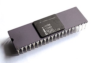
The chip was packaged in a (then unusual) 64-pin, 0.9" wide DIP. The comparatively large number of pins allowed for the 15-bit (word) address bus and 16-bit data bus to be brought out on dedicated pins without the use of multiplexing (unlike e.g. the Intel 8086 CPU), keeping external memory connections simple. Contrary to the convention used by many other manufacturers, TI labeled the most significant address and data lines "A0" and "D0", respectively. All internal data paths and the ALU are 16 bits wide.
The processor can be paused with the address bus tri-stated for external direct memory access (DMA). Memory accesses are always 16 bits wide, with the CPU automatically performing read-before-write operations for byte-wide accesses.
The hardware interrupt system supports a 4-bit interrupt priority input, which needed to be higher than the priority level stored in the status register (bits 12−15) in order for the interrupt request to be served. In addition, the /LOAD input provides a non-maskable interrupt facility with a dedicated vector.[8]
The TMS9900 CPU also contains a 16-bit shift register ("CRU") designed for interfacing with external shift registers, with dedicated instructions supporting access to fields of 1−16 bit width out of a total of 4096 addressable bits.
Parallel peripherals can be attached in memory-mapped fashion to the regular address and data bus.
Applications
The Tomy Tutor, a 1983 home computer based on the TMS9995 processor
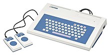
The TMS9900 was used in the TI-99/4 and TI-99/4A home computers. Unfortunately, to reduce the production costs, TI chose to use in these systems just 128 16-bit words of the fast kind of RAM that the TMS9900 could access directly. The rest of the memory was 16KB of 8-bitDRAM that was accessible only indirectly through the video display controller, which crippled the performance of the TI-99/4.
TI developed the TM990 series of computer modules, including CPU, memory, I/O, which when plugged into a card frame could form a 16-bit minicomputer. These were typically used for process control.[9] A microprocessor trainer was released in the form of the TM990/189.[10]
TMS9900 Family Product Development
The second generation of the TMS9900 family of microprocessors was the TMS9995 which provided "functional performance at speeds 3 times faster than any previous 9900 family processor",[11] largely due to the inclusion of instruction prefetch technology. In the home computer arena, the TMS9995 only found use in the Tomy Tutor, an esoteric TI99-4/A upgrade called the Geneve 9640, and a project printed in Electronics Today: the Powertran Cortex.[12] It was planned to be used in the TI-99/2 & TI-99/8 computer systems, but neither advanced past the prototype stage.
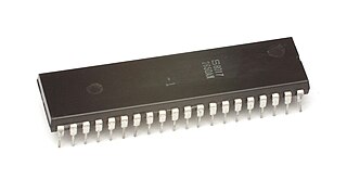
TMS9900NL in plastic DIP package
TI later developed the more powerful TMS99000 family of microprocessors, which was used as the CPU in the 990/10A minicomputer as a cost reduction. Unfortunately, by the time the 990/10A made it to market, the end of the minicomputer era was already in sight.
The TMS99000 family includes two microprocessors,[1] the TMS99105A and the TMS99110A, which are identical except for the contents of on-chip macrostore ROM memory (macrostore memory contains added functions or instructions through emulation routines written in standard machine code). The on-chip ROM Macrostore in the TMS99110A microprocessor contains floating point instructions which are available as part of the machine language instruction set, while the baseline TMS99105A does not. Both chips can implement Macrostore instructions in an external ROM. A third member of the TMS99000 family, the TMS99120, was announced[13] but may never have been commercially produced. The on-chip ROM Macrostore in the TMS99120 was to contain run-time support routines for the PASCAL high-level language.
The instruction set for the TMS99000 family extends the 9900 instruction set while keeping compatibility. The additional instructions includes those for signed multiply and divide (first appearing in the TMS9995), long-word shift, add, and subtract; load status register, load workspace pointer, stack operations, multiprocessor support, bit manipulation. Members of the family can access 256KB of memory through code/data segmentation, and may use the TIM99610 memory mapper to address up to 16MiB. The architecture contains many other advances over the TMS9900 and TMS9995.[1]
Variants
Model
Description
TI990/9
Early multi-chip CPU for minicomputer systems, 1974
TI990/10
Multi-chip implementation for minicomputer systems, 1975
TI990/12
Multi-chip implementation, faster than 990/10
TMS9900
Single chip implementation, 1976, used in the TI-99/4(A) computer
TMS9940
Microcontroller with 2KB ROM, 128B RAM, decrementer, CRU bus, 1979
TMS9980 TMS9981
8-bit databus versions of TMS9900
TMS9985
TMS9940 with 8KB ROM, 256B RAM, and an 8-bit external bus, c. 1978 (never released)
TMS9989
Improved 9980, used in military hardware
TMS9995
Improved TMS9985-like, no ROM. Used in the TI-99/2 & TI-99/8 prototypes, the Tomy Tutor and the Geneve computer Geneve 9640
TMS99105
Baseline member of the TMS99000 microprocessor family
TMS99110
TMS99000 family microprocessor with floating point instructions pre-programmed into the on-chip Macrostore ROM memory
TMS99120
TMS99000 family microprocessor with run-time support routines for the PASCAL high-level language pre-programmed into the on-chip Macrostore ROM memory (microprocessor was announced but may never have been commercially produced)
The Intel 8080 ("eighty-eighty") is the second 8-bit microprocessor designed and manufactured by Intel. It first appeared in April 1974 and is an extended and enhanced variant of the earlier 8008 design, although without binary compatibility. The initial specified clock rate or frequency limit was 2 MHz, with common instructions using 4, 5, 7, 10, or 11 cycles. As a result, the processor is able to execute several hundred thousand instructions per second. Two faster variants, the 8080A-1 and 8080A-2, became available later with clock frequency limits of 3.125 MHz and 2.63 MHz respectively. The 8080 needs two support chips to function in most applications: the i8224 clock generator/driver and the i8228 bus controller. It is implemented in N-type metal–oxide–semiconductor logic (NMOS) using non-saturated enhancement mode transistors as loads thus demanding a +12 V and a −5 V voltage in addition to the main transistor–transistor logic (TTL) compatible +5 V.
The 8086 is a 16-bit microprocessor chip designed by Intel between early 1976 and June 8, 1978, when it was released. The Intel 8088, released July 1, 1979, is a slightly modified chip with an external 8-bit data bus, and is notable as the processor used in the original IBM PC design.
The Motorola 68000 is a 16/32-bit complex instruction set computer (CISC) microprocessor, introduced in 1979 by Motorola Semiconductor Products Sector.
The Z80 is an 8-bit microprocessor introduced by Zilog as the startup company's first product. The Z80 was conceived by Federico Faggin in late 1974 and developed by him and his 11 employees starting in early 1975. The first working samples were delivered in March 1976, and it was officially introduced on the market in July 1976. With the revenue from the Z80, the company built its own chip factories and grew to over a thousand employees over the following two years.
The NS32000, sometimes known as the 32k, is a series of microprocessors produced by National Semiconductor. The first member of the family came to market in 1982, briefly known as the 16032 before becoming the 32016. It was the first general-purpose microprocessor on the market that used 32-bit data throughout: the Motorola 68000 used 32-bit data but had a 16-bit ALU and thus took twice as long perform many operations. However, the 32016 contained many bugs and often could not be run at its rated speed. These problems, and the presence of the otherwise similar 68000 which had been available since 1980, led to little use in the market.
The Intel MCS-51 is a single chip microcontroller (MCU) series developed by Intel in 1980 for use in embedded systems. The architect of the Intel MCS-51 instruction set was John H. Wharton. Intel's original versions were popular in the 1980s and early 1990s, and enhanced binary compatible derivatives remain popular today. It is a complex instruction set computer, but also has some of the features of RISC architectures, such as a large register set and register windows, and has separate memory spaces for program instructions and data.
The Intel 8085 ("eighty-eighty-five") is an 8-bit microprocessor produced by Intel and introduced in March 1976. It is software-binary compatible with the more-famous Intel 8080 with only two minor instructions added to support its added interrupt and serial input/output features. However, it requires less support circuitry, allowing simpler and less expensive microcomputer systems to be built. The "5" in the part number highlighted the fact that the 8085 uses a single +5-volt (V) power supply by using depletion-mode transistors, rather than requiring the +5 V, −5 V and +12 V supplies needed by the 8080. This capability matched that of the competing Z80, a popular 8080-derived CPU introduced the year before. These processors could be used in computers running the CP/M operating system.
The TI-99/4 and TI-99/4A are home computers released by Texas Instruments in 1979 and 1981, respectively. The TI-99 series competed against home computers such as the Apple II, TRS-80, Atari 400/800, and VIC-20.
The Clipper architecture is a 32-bit RISC-like instruction set architecture designed by Fairchild Semiconductor. The architecture never enjoyed much market success, and the only computer manufacturers to create major product lines using Clipper processors were Intergraph and High Level Hardware, although Opus Systems offered a product based on the Clipper as part of its Personal Mainframe range. The first processors using the Clipper architecture were designed and sold by Fairchild, but the division responsible for them was subsequently sold to Intergraph in 1987; Intergraph continued work on Clipper processors for use in its own systems.
The Signetics 2650 was an 8-bit microprocessor introduced in July 1975. According to Adam Osborne's book An Introduction to Microprocessors Vol 2: Some Real Products, it was "the most minicomputer-like" of the microprocessors available at the time. A combination of missing features and odd memory access limited its appeal, and the system saw little use in the market.
The TI-990 was a series of 16-bit minicomputers sold by Texas Instruments (TI) in the 1970s and 1980s. The TI-990 was a replacement for TI's earlier minicomputer systems, the TI-960 and the TI-980. It had several unique features, and was easier to program than its predecessors.
TLCS is a prefix applied to microcontrollers made by Toshiba. The product line includes multiple families of CISC and RISC architectures. Individual components generally have a part number beginning with "TMP". E.g. the TMP8048AP is a member of the TLCS-48 family.
The Intersil 6100 is a single-chip microprocessor implementation of the 12-bit PDP-8 instruction set, along with a range of peripheral support and memory ICs developed by Intersil in the mid-1970s. It was sometimes referred to as the CMOS-PDP8. Since it was also produced by Harris Corporation, it was also known as the Harris HM-6100. The Intersil 6100 was introduced in the second quarter of 1975, and the Harris version in 1976.
The CP1600 is a 16-bit microprocessor created in a partnership between General Instrument and Honeywell, introduced in February 1975. It is one of the first single-chip 16-bit processors. The overall design bears a strong resemblance to the PDP-11.
The PDP-11 architecture is a 16-bit CISC instruction set architecture (ISA) developed by Digital Equipment Corporation (DEC). It is implemented by central processing units (CPUs) and microprocessors used in PDP-11 minicomputers. It was in wide use during the 1970s, but was eventually overshadowed by the more powerful VAX architecture in the 1980s.
The ST6 and ST7 are 8-bit microcontroller product lines from STMicroelectronics. They are commonly used in small embedded applications like washing machines.
The Bellmac 32 is a microprocessor developed by Bell Labs' processor division in 1980, implemented using CMOS technology and was the first microprocessor that could move 32 bits in one clock cycle. The microprocessor contains 150,000 transistors and improved on the speed of CMOS design by using "domino circuits". It was designed with the C programming language in mind. After its creation, an improved version was produced called the Bellmac 32A, then cancelled along with its successor, the "Hobbit" C-language Reduced Instruction Set Processor (CRISP).
The Mostek MK5065 was an 8-bit microprocessor introduced by Mostek in early 1974. The design was originally developed by Motorola for use in an Olivetti electronic calculator, and was licensed to Mostek for use in non-calculator roles. It featured three sets of processor registers, allowing it to switch to an interrupt handler in a single cycle, and a wait-for-data mode that aided direct memory access.
The WD16 is a 16-bit microprocessor introduced by Western Digital in October 1976. It is based on the MCP-1600 chipset, a general-purpose design that was also used to implement the DEC LSI-11 low-end minicomputer and the Pascal MicroEngine processor. The three systems differed primarily in their microcode, giving each system a unique instruction set architecture (ISA).
The COP400 or COP II is a 4-bit microcontroller family introduced in 1977 by National Semiconductor as a follow-on product to their original PMOS COP microcontroller. COP400 family members are complete microcomputers containing internal timing, logic, ROM, RAM, and I/O necessary to implement dedicated controllers. Some COP400 devices were second-sourced by Western Digital as the WD4200 family. In the Soviet Union several COP400 microcontrollers were manufactured as the 1820 series.
This page is based on this Wikipedia article Text is available under the CC BY-SA 4.0 license; additional terms may apply. Images, videos and audio are available under their respective licenses.