Shift register

Last updated

A shift register is a type of digital circuit using a cascade of flip-flops where the output of one flip-flop is connected to the input of the next. They share a single clock signal, which causes the data stored in the system to shift from one location to the next. By connecting the last flip-flop back to the first, the data can cycle within the shifters for extended periods, and in this configuration they were used as computer memory, displacing delay-line memory systems in the late 1960s and early 1970s.

Contents

In most cases, several parallel shift registers would be used to build a larger memory pool known as a "bit array". Data was stored into the array and read back out in parallel, often as a computer word, while each bit was stored serially in the shift registers. There is an inherent trade-off in the design of bit arrays; putting more flip-flops in a row allows a single shifter to store more bits, but requires more clock cycles to push the data through all of the shifters before the data can be read back out again.

Shift registers can have both parallel and serial inputs and outputs. These are often configured as "serial-in, parallel-out" (SIPO) or as "parallel-in, serial-out" (PISO). There are also types that have both serial and parallel input and types with serial and parallel output. There are also "bidirectional" shift registers, which allow shifting in both directions: L  R or R  L. The serial input and last output of a shift register can also be connected to create a "circular shift register". A PIPO register (parallel in, parallel out) is simply a D-type register and is not a shift register, but is very fast – an output is given within a single clock pulse. A "universal" shift register provides bidirectional serial-in and serial-out, as well as parallel-in and parallel-out.

Serial-in serial-out (SISO)

Destructive readout

Sample usage of a 4-bit shift register. Data input is 10110000.
Time
Output 1
Output 2
Output 3
Output 4
00000
11000
20100
31010
41101
50110
60011
70001
80000

These are the simplest kind of shift registers. The data string is presented at "data in" and is shifted right one stage each time "data advance" is brought high. At each advance, the bit on the far left (i.e. "data in") is shifted into the first flip-flop's output. The bit on the far right (i.e. "data out") is shifted out and lost.

The data is stored after each flip-flop on the "Q" output, so there are four storage "slots" available in this arrangement, hence it is a 4-bit register. To give an idea of the shifting pattern, imagine that the register holds 0000 (so all storage slots are empty). As "data in" presents 1,0,1,1,0,0,0,0 (in that order, with a pulse at "data advance" each time—this is called clocking or strobing) to the register, this is the result. The right hand column corresponds to the right-most flip-flop's output pin, and so on.

So the serial output of the entire register is 00010110. It can be seen that if data were to be continued to input, it would get exactly what was put in (10110000), but offset by four "data advance" cycles. This arrangement is the hardware equivalent of a queue. Also, at any time, the whole register can be set to zero by bringing the reset (R) pins high.

This arrangement performs destructive readout  each datum is lost once it has been shifted out of the right-most bit.

Serial-in parallel-out (SIPO)

4-Bit SIPO Shift Register.svg

This configuration allows conversion from serial to parallel format. Data input is serial, as described in the SISO section above. Once the data has been clocked in, it may be either read off at each output simultaneously, or it can be shifted out.

In this configuration, each flip-flop is edge triggered. All flip-flops operate at the given clock frequency. Each input bit makes its way down to the Nth output after N clock cycles, leading to parallel output.

In cases where the parallel outputs should not change during the serial loading process, it's desirable to use a latched or buffered output. In a latched shift register (such as the 74595) the serial data is first loaded into an internal buffer register, then upon receipt of a load signal the state of the buffer register is copied into a set of output registers. In general, the practical application of the serial-in/parallel-out shift register is to convert data from serial format on a single wire to parallel format on multiple wires.

Parallel-in serial-out (PISO)

This configuration has the data input on lines D1 through D4 in parallel format, D1 being the most significant bit. To write the data to the register, the Write/Shift control line must be held LOW. To shift the data, the W/S control line is brought HIGH and the registers are clocked. The arrangement now acts as a PISO shift register, with D1 as the Data Input. However, as long as the number of clock cycles is not more than the length of the data-string, the Data Output, Q, will be the parallel data read off in order.

4-Bit PISO Shift Register 4-Bit PISO Shift Register.png
4-Bit PISO Shift Register

The animation below shows the write/shift sequence, including the internal state of the shift register.

4-Bit PISO Shift Register Seq.gif

Uses

Toshiba TC4015BP dual SIPO shift register DOV-1X - Toshiba TC4015BP on printed circuit board-9788.jpg
Toshiba TC4015BP dual SIPO shift register

Serial and parallel conversion

One of the most common uses of a shift register is to convert between serial and parallel interfaces.

Delay

Serial-in serial-out shift registers can be used as simple delay circuits. [1]

Stack

Several bidirectional shift registers can also be connected in parallel for a hardware implementation of a stack.

More I/O pins

Shift registers are commonly attached to microcontrollers when more general-purpose input/output pins are required than are available, sometimes over a Serial Peripheral Interface in daisy chain configuration, which allows any number of binary devices to be accessed using only two to four pins, though more slowly than parallel I/O.

For more outputs, SIPO shift registers are used. The parallel outputs of the shift register and the desired state for all those devices can be sent out of the microcontroller using a single serial connection.

For more inputs, PISO shift registers are used. Each binary input (such as a button or more complicated circuitry) is attached to a parallel input of the shift register, then the data is sent back serially to the microcontroller.

Pulse extenders

Shift registers can also be used as pulse extenders. Compared to monostable multivibrators, the timing does not depend on component values, but it requires an external clock, and the timing accuracy is limited by the granularity of this clock. An example of such a pulse extender is the Ronja Twister, wherein five 74164 shift registers create the core of the timing logic this way (schematic).

Data processing

In early computers, shift registers were used to handle data processing: two numbers to be added were stored in two shift registers and clocked out into an arithmetic and logic unit (ALU) with the result being fed back to the input of one of the shift registers (the accumulator), which was one bit longer, since binary addition can only result in an answer that has the same size or is one bit longer.

Bitshift operations

Many computer languages include bitwise operations to "shift right" and "shift left" the data in a register, effectively dividing by two or multiplying by two for each place shifted.

Shift register memory

Very large serial-in serial-out shift registers (thousands of bits in size) were used in a similar manner to the earlier delay-line memory in some devices built in the early 1970s. Shift registers don't need many pins or address decoding logic, so was much cheaper than random-access memory back then. [2] Such shift register memory was sometimes called circulating memory.

Datapoint 3300, for example, stored its terminal display of 25 rows of 72 columns of 6-bit upper-case characters using 54 200-bit shift registers (arranged in 6 tracks of 9 packs), providing storage for 1800 characters. The shift register design meant that scrolling the terminal display could be accomplished by simply pausing the display output to skip one line of characters. [3] A similar design was used for the Apple I's terminal. [4]

History

One of the first known examples of a shift register was in the Mark 2 Colossus, a code-breaking machine built in 1944. It was a six-stage device built of vacuum tubes and thyratrons. [5] A shift register was also used in the IAS machine, built by John von Neumann and others at the Institute for Advanced Study in the late 1940s. Shift registers made their way into integrated circuits in the 1960s as evidenced by early patents from Frank Wanlass [6] and Kent Smith [7] working at General Instrument.

See also

Related Research Articles

In digital logic and computing, a counter is a device which stores the number of times a particular event or process has occurred, often in relationship to a clock. The most common type is a sequential digital logic circuit with an input line called the clock and multiple output lines. The values on the output lines represent a number in the binary or BCD number system. Each pulse applied to the clock input increments or decrements the number in the counter.

<span class="mw-page-title-main">Microcontroller</span> Small computer on a single integrated circuit

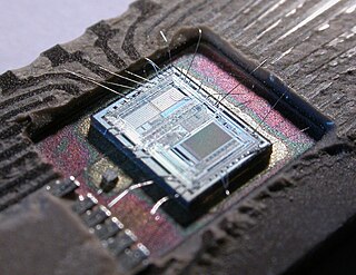
A microcontroller or microcontroller unit (MCU) is a small computer on a single integrated circuit. A microcontroller contains one or more CPUs along with memory and programmable input/output peripherals. Program memory in the form of NOR flash, OTP ROM or ferroelectric RAM is also often included on chip, as well as a small amount of RAM. Microcontrollers are designed for embedded applications, in contrast to the microprocessors used in personal computers or other general purpose applications consisting of various discrete chips.

<span class="mw-page-title-main">Universal asynchronous receiver-transmitter</span> Computer hardware device

A universal asynchronous receiver-transmitter is a peripheral device for asynchronous serial communication in which the data format and transmission speeds are configurable. It sends data bits one by one, from the least significant to the most significant, framed by start and stop bits so that precise timing is handled by the communication channel. The electric signaling levels are handled by a driver circuit external to the UART. Common signal levels are RS-232, RS-485, and raw TTL for short debugging links. Early teletypewriters used current loops.

<span class="mw-page-title-main">Intel 8085</span> 8-bit microprocessor by Intel

The Intel 8085 ("eighty-eighty-five") is an 8-bit microprocessor produced by Intel and introduced in March 1976. It is the last 8-bit microprocessor developed by Intel.

<span class="mw-page-title-main">AVR microcontrollers</span> Family of microcontrollers

AVR is a family of microcontrollers developed since 1996 by Atmel, acquired by Microchip Technology in 2016. These are modified Harvard architecture 8-bit RISC single-chip microcontrollers. AVR was one of the first microcontroller families to use on-chip flash memory for program storage, as opposed to one-time programmable ROM, EPROM, or EEPROM used by other microcontrollers at the time.

<span class="mw-page-title-main">TI MSP430</span> Mixed-signal microcontroller family

The MSP430 is a mixed-signal microcontroller family from Texas Instruments, first introduced on 14 February 1992. Built around a 16-bit CPU, the MSP430 was designed for low power consumption embedded applications and low cost.

Serial Peripheral Interface (SPI) is a de facto standard for synchronous serial communication, used primarily in embedded systems for short-distance wired communication between integrated circuits.

JTAG is an industry standard for verifying designs of and testing printed circuit boards after manufacture.

<span class="mw-page-title-main">MOS Technology 6522</span> Microprocessor I/O port controller IC

The MOS Technology 6522 Versatile Interface Adapter (VIA) is an integrated circuit that was designed and manufactured by MOS Technology as an I/O port controller for the 6502 family of microprocessors. It provides two bidirectional 8-bit parallel I/O ports, two 16-bit timers, and an 8-bit shift register for serial communications or data conversion between serial and parallel forms. The direction of each bit of the two I/O ports can be individually programmed. In addition to being manufactured by MOS Technology, the 6522 was second sourced by other companies including Rockwell and Synertek.

A general-purpose input/output (GPIO) is an uncommitted digital signal pin on an integrated circuit or electronic circuit board which may be used as an input or output, or both, and is controllable by software.

Clock skew is a phenomenon in synchronous digital circuit systems in which the same sourced clock signal arrives at different components at different times due to gate or, in more advanced semiconductor technology, wire signal propagation delay. The instantaneous difference between the readings of any two clocks is called their skew.

XDR DRAM is a high-performance dynamic random-access memory interface. It is based on and succeeds RDRAM. Competing technologies include DDR2 and GDDR4.

The original Macintosh was a relatively simple machine, now of interest for its simplicity and for the fact that it was the first computer produced by Apple under the name Macintosh. The Macintosh used standard off-the-shelf components to the greatest extent possible, achieving a moderate price point by mixing complex LSI chips, readily customizable programmable array logic, and off-the-shelf components.

A Serializer/Deserializer (SerDes) is a pair of functional blocks commonly used in high speed communications to compensate for limited input/output. These blocks convert data between serial data and parallel interfaces in each direction. The term "SerDes" generically refers to interfaces used in various technologies and applications. The primary use of a SerDes is to provide data transmission over a single line or a differential pair in order to minimize the number of I/O pins and interconnects.

<span class="mw-page-title-main">Intel 8255</span> Programmable Peripheral Interface chip

The Intel 8255 Programmable Peripheral Interface (PPI) chip was developed and manufactured by Intel in the first half of the 1970s for the Intel 8080 microprocessor. The 8255 provides 24 parallel input/output lines with a variety of programmable operating modes.

<span class="mw-page-title-main">Single-board microcontroller</span> Microcontroller built onto a single printed circuit board

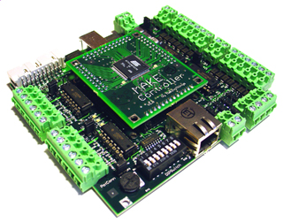
A single-board microcontroller is a microcontroller built onto a single printed circuit board. This board provides all of the circuitry necessary for a useful control task: a microprocessor, I/O circuits, a clock generator, RAM, stored program memory and any necessary support ICs. The intention is that the board is immediately useful to an application developer, without requiring them to spend time and effort to develop controller hardware.

<span class="mw-page-title-main">Flip-flop (electronics)</span> Electronic circuit with two stable states

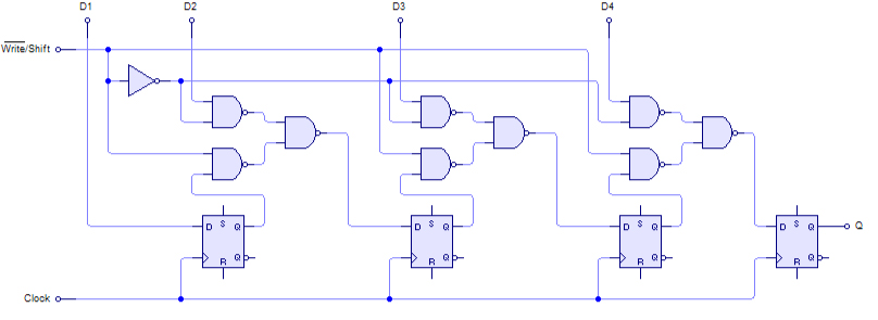
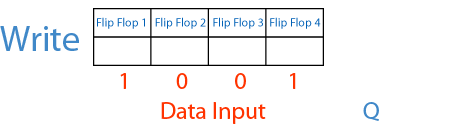
In electronics, flip-flops and latches are circuits that have two stable states that can store state information – a bistable multivibrator. The circuit can be made to change state by signals applied to one or more control inputs and will output its state. It is the basic storage element in sequential logic. Flip-flops and latches are fundamental building blocks of digital electronics systems used in computers, communications, and many other types of systems.

<span class="mw-page-title-main">Signetics 8X300</span> Signetics microprocessor

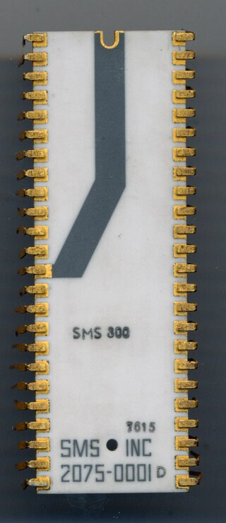
The 8X300 is a microprocessor produced and marketed by Signetics starting 1976 as a second source for the SMS 300 by Scientific Micro Systems, Inc. Although SMS developed the SMS 300, Signetics was the sole manufacturer of this product line. In 1978 Signetics purchased the rights to the SMS 300 series and renamed it 8X300.

<span class="mw-page-title-main">COP400</span> 4-bit microcontroller family

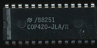
The COP400 or COP II is a 4-bit microcontroller family introduced in 1977 by National Semiconductor as a follow-on product to their original PMOS COP microcontroller. COP400 family members are complete microcomputers containing internal timing, logic, ROM, RAM, and I/O necessary to implement dedicated controllers. Some COP400 devices were second-sourced by Western Digital as the WD4200 family. In the Soviet Union several COP400 microcontrollers were manufactured as the 1820 series.

References

  1. US4530107A,Williams, Marshall,"Shift register delay circuit",issued 1985-07-16
  2. Shirriff, Ken (2014). "Inside the Intel 1405: die photos of a shift register memory from 1970". Ken Shirriff's blog. Archived from the original on 2023-07-28. Retrieved 2023-08-06.
  3. "DataPoint 3300 Maintenance Manual" (PDF). bitsavers.org. Datapoint Corporation. December 1976.
  4. Shirriff, Ken. "Inside the Apple-1's shift-register memory". Ken Shirriff's blog. Archived from the original on 2023-06-06. Retrieved 2023-08-04.
  5. Flowers, Thomas H. (1983), "The Design of Colossus", Annals of the History of Computing, 5 (3): 246, doi:10.1109/MAHC.1983.10079, S2CID   39816473
  6. "Shift register system".
  7. "Electronic shift register system".