Related Research Articles
Instructions per second (IPS) is a measure of a computer's processor speed. For complex instruction set computers (CISCs), different instructions take different amounts of time, so the value measured depends on the instruction mix; even for comparing processors in the same family the IPS measurement can be problematic. Many reported IPS values have represented "peak" execution rates on artificial instruction sequences with few branches and no cache contention, whereas realistic workloads typically lead to significantly lower IPS values. Memory hierarchy also greatly affects processor performance, an issue barely considered in IPS calculations. Because of these problems, synthetic benchmarks such as Dhrystone are now generally used to estimate computer performance in commonly used applications, and raw IPS has fallen into disuse.
x86 is a family of complex instruction set computer (CISC) instruction set architectures initially developed by Intel based on the Intel 8086 microprocessor and its 8088 variant. The 8086 was introduced in 1978 as a fully 16-bit extension of Intel's 8-bit 8080 microprocessor, with memory segmentation as a solution for addressing more memory than can be covered by a plain 16-bit address. The term "x86" came into being because the names of several successors to Intel's 8086 processor end in "86", including the 80186, 80286, 80386 and 80486 processors.
In computing, Streaming SIMD Extensions (SSE) is a single instruction, multiple data (SIMD) instruction set extension to the x86 architecture, designed by Intel and introduced in 1999 in their Pentium III series of Central processing units (CPUs) shortly after the appearance of Advanced Micro Devices (AMD's) 3DNow!. SSE contains 70 new instructions, most of which work on single precision floating-point data. SIMD instructions can greatly increase performance when exactly the same operations are to be performed on multiple data objects. Typical applications are digital signal processing and graphics processing.

In computing, floating point operations per second is a measure of computer performance, useful in fields of scientific computations that require floating-point calculations. For such cases, it is a more accurate measure than measuring instructions per second.

IA-64 is the instruction set architecture (ISA) of the Itanium family of 64-bit Intel microprocessors. The basic ISA specification originated at Hewlett-Packard (HP), and was subsequently implemented by Intel in collaboration with HP. The first Itanium processor, codenamed Merced, was released in 2001.
The Pentium Pro is a sixth-generation x86 microprocessor developed and manufactured by Intel and introduced on November 1, 1995. It introduced the P6 microarchitecture and was originally intended to replace the original Pentium in a full range of applications. While the Pentium and Pentium MMX had 3.1 and 4.5 million transistors, respectively, the Pentium Pro contained 5.5 million transistors. Later, it was reduced to a more narrow role as a server and high-end desktop processor and was used in supercomputers like ASCI Red, the first computer to reach the trillion floating point operations per second (teraFLOPS) performance mark. The Pentium Pro was capable of both dual- and quad-processor configurations. It only came in one form factor, the relatively large rectangular Socket 8. The Pentium Pro was succeeded by the Pentium II Xeon in 1998.
SSE2 is one of the Intel SIMD processor supplementary instruction sets first introduced by Intel with the initial version of the Pentium 4 in 2000. It extends the earlier SSE instruction set, and is intended to fully replace MMX. Intel extended SSE2 to create SSE3 in 2004. SSE2 added 144 new instructions to SSE, which has 70 instructions. Competing chip-maker AMD added support for SSE2 with the introduction of their Opteron and Athlon 64 ranges of AMD64 64-bit CPUs in 2003.

A coprocessor is a computer processor used to supplement the functions of the primary processor. Operations performed by the coprocessor may be floating-point arithmetic, graphics, signal processing, string processing, cryptography or I/O interfacing with peripheral devices. By offloading processor-intensive tasks from the main processor, coprocessors can accelerate system performance. Coprocessors allow a line of computers to be customized, so that customers who do not need the extra performance do not need to pay for it.
In computing, especially digital signal processing, the multiply–accumulate (MAC) or multiply-add (MAD) operation is a common step that computes the product of two numbers and adds that product to an accumulator. The hardware unit that performs the operation is known as a multiplier–accumulator ; the operation itself is also often called a MAC or a MAD operation. The MAC operation modifies an accumulator a:
A processor register is a quickly accessible location available to a computer's processor. Registers usually consist of a small amount of fast storage, although some registers have specific hardware functions, and may be read-only or write-only. In computer architecture, registers are typically addressed by mechanisms other than main memory, but may in some cases be assigned a memory address e.g. DEC PDP-10, ICT 1900.
Cell is a multi-core microprocessor microarchitecture that combines a general-purpose PowerPC core of modest performance with streamlined coprocessing elements which greatly accelerate multimedia and vector processing applications, as well as many other forms of dedicated computation.

POWER7 is a family of superscalar multi-core microprocessors based on the Power ISA 2.06 instruction set architecture released in 2010 that succeeded the POWER6 and POWER6+. POWER7 was developed by IBM at several sites including IBM's Rochester, MN; Austin, TX; Essex Junction, VT; T. J. Watson Research Center, NY; Bromont, QC and IBM Deutschland Research & Development GmbH, Böblingen, Germany laboratories. IBM announced servers based on POWER7 on 8 February 2010.

Tesla is the codename for a GPU microarchitecture developed by Nvidia, and released in 2006, as the successor to Curie microarchitecture. It was named after the pioneering electrical engineer Nikola Tesla. As Nvidia's first microarchitecture to implement unified shaders, it was used with GeForce 8 Series, GeForce 9 Series, GeForce 100 Series, GeForce 200 Series, and GeForce 300 Series of GPUs collectively manufactured in 90 nm, 80 nm, 65 nm, 55 nm, and 40 nm. It was also in the GeForce 405 and in the Quadro FX, Quadro x000, Quadro NVS series, and Nvidia Tesla computing modules.
Intel Teraflops Research Chip is a research manycore processor containing 80 cores, using a network-on-chip architecture, developed by Intel's Tera-Scale Computing Research Program. It was manufactured using a 65 nm CMOS process with eight layers of copper interconnect and contains 100 million transistors on a 275 mm2 die. Its design goal was to demonstrate a modular architecture capable of a sustained performance of 1.0 TFLOPS while dissipating less than 100 W. Research from the project was later incorporated into Xeon Phi. The technical lead of the project was Sriram R. Vangal.
AMD FireStream was AMD's brand name for their Radeon-based product line targeting stream processing and/or GPGPU in supercomputers. Originally developed by ATI Technologies around the Radeon X1900 XTX in 2006, the product line was previously branded as both ATI FireSTREAM and AMD Stream Processor. The AMD FireStream can also be used as a floating-point co-processor for offloading CPU calculations, which is part of the Torrenza initiative. The FireStream line has been discontinued since 2012, when GPGPU workloads were entirely folded into the AMD FirePro line.
The SSE5 was a SIMD instruction set extension proposed by AMD on August 30, 2007 as a supplement to the 128-bit SSE core instructions in the AMD64 architecture.
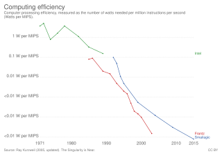
In computing, performance per watt is a measure of the energy efficiency of a particular computer architecture or computer hardware. Literally, it measures the rate of computation that can be delivered by a computer for every watt of power consumed. This rate is typically measured by performance on the LINPACK benchmark when trying to compare between computing systems: an example using this is the Green500 list of supercomputers. Performance per watt has been suggested to be a more sustainable measure of computing than Moore’s Law.
Advanced Vector Extensions (AVX) are extensions to the x86 instruction set architecture for microprocessors from Intel and Advanced Micro Devices (AMD). They were proposed by Intel in March 2008 and first supported by Intel with the Sandy Bridge processor shipping in Q1 2011 and later by AMD with the Bulldozer processor shipping in Q3 2011. AVX provides new features, new instructions and a new coding scheme.
Petascale computing refers to computing systems capable of calculating at least 1015 floating point operations per second (1 petaFLOPS). Petascale computing allowed faster processing of traditional supercomputer applications. The first system to reach this milestone was the IBM Roadrunner in 2008. Petascale supercomputers are planned to be succeeded by exascale computers.

Xeon Phi was a series of x86 manycore processors designed and made by Intel. It was intended for use in supercomputers, servers, and high-end workstations. Its architecture allowed use of standard programming languages and application programming interfaces (APIs) such as OpenMP.
References
- ↑ "Practitioner's guide to adjusted peak performance". U.S. Department of Commerce - Bureau of Industry and Security. December 2006. Archived from the original on 2019-10-07.