Electronegativity, symbol χ, measures the tendency of an atom to attract a shared pair of electrons. An atom's electronegativity is affected by both its atomic number and the distance at which its valence electrons reside from the charged nucleus. The higher the associated electronegativity, the more an atom or a substituent group attracts electrons.
In solid-state physics, the work function is the minimum thermodynamic work needed to remove an electron from a solid to a point in the vacuum immediately outside the solid surface. Here "immediately" means that the final electron position is far from the surface on the atomic scale, but still too close to the solid to be influenced by ambient electric fields in the vacuum. The work function is not a characteristic of a bulk material, but rather a property of the surface of the material.
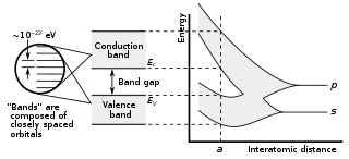
In solid-state physics, a band gap, also called an energy gap, is an energy range in a solid where no electronic states can exist. In graphs of the electronic band structure of solids, the band gap generally refers to the energy difference between the top of the valence band and the bottom of the conduction band in insulators and semiconductors. It is the energy required to promote a valence electron bound to an atom to become a conduction electron, which is free to move within the crystal lattice and serve as a charge carrier to conduct electric current. It is closely related to the HOMO/LUMO gap in chemistry. If the valence band is completely full and the conduction band is completely empty, then electrons cannot move in the solid; however, if some electrons transfer from the valence to the conduction band, then current can flow. Therefore, the band gap is a major factor determining the electrical conductivity of a solid. Substances with large band gaps are generally insulators, those with smaller band gaps are semiconductors, while conductors either have very small band gaps or none, because the valence and conduction bands overlap.
The electron affinity (Eea) of an atom or molecule is defined as the amount of energy released when an electron is attached to a neutral atom or molecule in the gaseous state to form a negative ion.

A Schottky barrier, named after Walter H. Schottky, is a potential energy barrier for electrons formed at a metal–semiconductor junction. Schottky barriers have rectifying characteristics, suitable for use as a diode. One of the primary characteristics of a Schottky barrier is the Schottky barrier height, denoted by ΦB. The value of ΦB depends on the combination of metal and semiconductor.
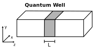
A quantum well is a potential well with only discrete energy values.
A heterojunction is an interface that occurs between two layers or regions of dissimilar semiconductors. These semiconducting materials have unequal band gaps as opposed to a homojunction. It is often advantageous to engineer the electronic energy bands in many solid-state device applications, including semiconductor lasers, solar cells and transistors. The combination of multiple heterojunctions together in a device is called a heterostructure, although the two terms are commonly used interchangeably. The requirement that each material be a semiconductor with unequal band gaps is somewhat loose, especially on small length scales, where electronic properties depend on spatial properties. A more modern definition of heterojunction is the interface between any two solid-state materials, including crystalline and amorphous structures of metallic, insulating, fast ion conductor and semiconducting materials.

A high-electron-mobility transistor (HEMT), also known as heterostructure FET (HFET) or modulation-doped FET (MODFET), is a field-effect transistor incorporating a junction between two materials with different band gaps as the channel instead of a doped region. A commonly used material combination is GaAs with AlGaAs, though there is wide variation, dependent on the application of the device. Devices incorporating more indium generally show better high-frequency performance, while in recent years, gallium nitride HEMTs have attracted attention due to their high-power performance. Like other FETs, HEMTs are used in integrated circuits as digital on-off switches. FETs can also be used as amplifiers for large amounts of current using a small voltage as a control signal. Both of these uses are made possible by the FET’s unique current–voltage characteristics. HEMT transistors are able to operate at higher frequencies than ordinary transistors, up to millimeter wave frequencies, and are used in high-frequency products such as cell phones, satellite television receivers, voltage converters, and radar equipment. They are widely used in satellite receivers, in low power amplifiers and in the defense industry.
In semiconductor production, doping is the intentional introduction of impurities into an intrinsic semiconductor for the purpose of modulating its electrical, optical and structural properties. The doped material is referred to as an extrinsic semiconductor. A semiconductor doped to such high levels that it acts more like a conductor than a semiconductor is referred to as a degenerate semiconductor.
In quantum physics, Fermi's golden rule is a formula that describes the transition rate from one energy eigenstate of a quantum system to a group of energy eigenstates in a continuum, as a result of a weak perturbation. This transition rate is effectively independent of time and is proportional to the strength of the coupling between the initial and final states of the system as well as the density of states. It is also applicable when the final state is discrete, i.e. it is not part of a continuum, if there is some decoherence in the process, like relaxation or collision of the atoms, or like noise in the perturbation, in which case the density of states is replaced by the reciprocal of the decoherence bandwidth.
In the solid-state physics of semiconductors, carrier generation and carrier recombination are processes by which mobile charge carriers are created and eliminated. Carrier generation and recombination processes are fundamental to the operation of many optoelectronic semiconductor devices, such as photodiodes, light-emitting diodes and laser diodes. They are also critical to a full analysis of p-n junction devices such as bipolar junction transistors and p-n junction diodes.

In solid-state physics of semiconductors, a band diagram is a diagram plotting various key electron energy levels as a function of some spatial dimension, which is often denoted x. These diagrams help to explain the operation of many kinds of semiconductor devices and to visualize how bands change with position. The bands may be coloured to distinguish level filling.
Band offset describes the relative alignment of the energy bands at a semiconductor heterojunction.
In solid-state physics, a metal–semiconductor (M–S) junction is a type of electrical junction in which a metal comes in close contact with a semiconductor material. It is the oldest practical semiconductor device. M–S junctions can either be rectifying or non-rectifying. The rectifying metal–semiconductor junction forms a Schottky barrier, making a device known as a Schottky diode, while the non-rectifying junction is called an ohmic contact.
In bulk semiconductor band structure calculations, it is assumed that the crystal lattice of the material is infinite. When the finite size of a crystal is taken into account, the wavefunctions of electrons are altered and states that are forbidden within the bulk semiconductor gap are allowed at the surface. Similarly, when a metal is deposited onto a semiconductor, the wavefunction of an electron in the semiconductor must match that of an electron in the metal at the interface. Since the Fermi levels of the two materials must match at the interface, there exists gap states that decay deeper into the semiconductor.
A quasi Fermi level is a term used in quantum mechanics and especially in solid state physics for the Fermi level that describes the population of electrons separately in the conduction band and valence band, when their populations are displaced from equilibrium. This displacement could be caused by the application of an external voltage, or by exposure to light of energy , which alter the populations of electrons in the conduction band and valence band. Since recombination rate tends to be much slower than the energy relaxation rate within each band, the conduction band and valence band can each have an individual population that is internally in equilibrium, even though the bands are not in equilibrium with respect to exchange of electrons. The displacement from equilibrium is such that the carrier populations can no longer be described by a single Fermi level, however it is possible to describe using concept of separate quasi-Fermi levels for each band.
Defect types include atom vacancies, adatoms, steps, and kinks that occur most frequently at surfaces due to the finite material size causing crystal discontinuity. What all types of defects have in common, whether surface or bulk defects, is that they produce dangling bonds that have specific electron energy levels different from those of the bulk. This difference occurs because these states cannot be described with periodic Bloch waves due to the change in electron potential energy caused by the missing ion cores just outside the surface. Hence, these are localized states that require separate solutions to the Schrödinger equation so that electron energies can be properly described. The break in periodicity results in a decrease in conductivity due to defect scattering.

In semiconductor physics, the band gap of a semiconductor can be of two basic types, a direct band gap or an indirect band gap. The minimal-energy state in the conduction band and the maximal-energy state in the valence band are each characterized by a certain crystal momentum (k-vector) in the Brillouin zone. If the k-vectors are different, the material has an "indirect gap". The band gap is called "direct" if the crystal momentum of electrons and holes is the same in both the conduction band and the valence band; an electron can directly emit a photon. In an "indirect" gap, a photon cannot be emitted because the electron must pass through an intermediate state and transfer momentum to the crystal lattice.
Free carrier absorption occurs when a material absorbs a photon, and a carrier is excited from an already-excited state to another, unoccupied state in the same band. This intraband absorption is different from interband absorption because the excited carrier is already in an excited band, such as an electron in the conduction band or a hole in the valence band, where it is free to move. In interband absorption, the carrier starts in a fixed, nonconducting band and is excited to a conducting one.
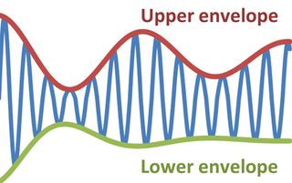
In physics and engineering, the envelope of an oscillating signal is a smooth curve outlining its extremes. The envelope thus generalizes the concept of a constant amplitude into an instantaneous amplitude. The figure illustrates a modulated sine wave varying between an upper and a lower envelope. The envelope function may be a function of time, space, angle, or indeed of any variable.


