The photoelectric effect is the emission of electrons when electromagnetic radiation, such as light, hits a material. Electrons emitted in this manner are called photoelectrons. The phenomenon is studied in condensed matter physics, solid state, and quantum chemistry to draw inferences about the properties of atoms, molecules and solids. The effect has found use in electronic devices specialized for light detection and precisely timed electron emission.
In solid-state physics, the work function is the minimum thermodynamic work needed to remove an electron from a solid to a point in the vacuum immediately outside the solid surface. Here "immediately" means that the final electron position is far from the surface on the atomic scale, but still too close to the solid to be influenced by ambient electric fields in the vacuum. The work function is not a characteristic of a bulk material, but rather a property of the surface of the material.

Surface science is the study of physical and chemical phenomena that occur at the interface of two phases, including solid–liquid interfaces, solid–gas interfaces, solid–vacuum interfaces, and liquid–gas interfaces. It includes the fields of surface chemistry and surface physics. Some related practical applications are classed as surface engineering. The science encompasses concepts such as heterogeneous catalysis, semiconductor device fabrication, fuel cells, self-assembled monolayers, and adhesives. Surface science is closely related to interface and colloid science. Interfacial chemistry and physics are common subjects for both. The methods are different. In addition, interface and colloid science studies macroscopic phenomena that occur in heterogeneous systems due to peculiarities of interfaces.

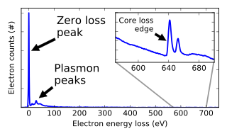
Electron energy loss spectroscopy (EELS) is a form of electron microscopy in which a material is exposed to a beam of electrons with a known, narrow range of kinetic energies. Some of the electrons will undergo inelastic scattering, which means that they lose energy and have their paths slightly and randomly deflected. The amount of energy loss can be measured via an electron spectrometer and interpreted in terms of what caused the energy loss. Inelastic interactions include phonon excitations, inter- and intra-band transitions, plasmon excitations, inner shell ionizations, and Cherenkov radiation. The inner-shell ionizations are particularly useful for detecting the elemental components of a material. For example, one might find that a larger-than-expected number of electrons comes through the material with 285 eV less energy than they had when they entered the material. This is approximately the amount of energy needed to remove an inner-shell electron from a carbon atom, which can be taken as evidence that there is a significant amount of carbon present in the sample. With some care, and looking at a wide range of energy losses, one can determine the types of atoms, and the numbers of atoms of each type, being struck by the beam. The scattering angle can also be measured, giving information about the dispersion relation of whatever material excitation caused the inelastic scattering.

In physics, a plasmon is a quantum of plasma oscillation. Just as light consists of photons, the plasma oscillation consists of plasmons. The plasmon can be considered as a quasiparticle since it arises from the quantization of plasma oscillations, just like phonons are quantizations of mechanical vibrations. Thus, plasmons are collective oscillations of the free electron gas density. For example, at optical frequencies, plasmons can couple with a photon to create another quasiparticle called a plasmon polariton.

Electron ionization is an ionization method in which energetic electrons interact with solid or gas phase atoms or molecules to produce ions. EI was one of the first ionization techniques developed for mass spectrometry. However, this method is still a popular ionization technique. This technique is considered a hard ionization method, since it uses highly energetic electrons to produce ions. This leads to extensive fragmentation, which can be helpful for structure determination of unknown compounds. EI is the most useful for organic compounds which have a molecular weight below 600. Also, several other thermally stable and volatile compounds in solid, liquid and gas states can be detected with the use of this technique when coupled with various separation methods.

Molecular-beam epitaxy (MBE) is an epitaxy method for thin-film deposition of single crystals. MBE is widely used in the manufacture of semiconductor devices, including transistors, and it is considered one of the fundamental tools for the development of nanotechnologies. MBE is used to fabricate diodes and MOSFETs at microwave frequencies, and to manufacture the lasers used to read optical discs.

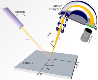
Photoemission spectroscopy (PES), also known as photoelectron spectroscopy, refers to energy measurement of electrons emitted from solids, gases or liquids by the photoelectric effect, in order to determine the binding energies of electrons in the substance. The term refers to various techniques, depending on whether the ionization energy is provided by X-ray, XUV or UV photons. Regardless of the incident photon beam, however, all photoelectron spectroscopy revolves around the general theme of surface analysis by measuring the ejected electrons.

In chemistry, a dangling bond is an unsatisfied valence on an immobilized atom. An atom with a dangling bond is also referred to as an immobilized free radical or an immobilized radical, a reference to its structural and chemical similarity to a free radical.

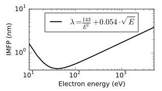
The inelastic mean free path (IMFP) is an index of how far an electron on average travels through a solid before losing energy.

Extreme ultraviolet radiation or high-energy ultraviolet radiation is electromagnetic radiation in the part of the electromagnetic spectrum spanning wavelengths shorter that the hydrogen Lyman-alpha line from 121 nm down to the X-ray band of 10 nm, and therefore having photons with energies from 10.26 eV up to 124.24 eV. EUV is naturally generated by the solar corona and artificially by plasma, high harmonic generation sources and synchrotron light sources. Since UVC extends to 100 nm, there is some overlap in the terms.

Anderson's rule is used for the construction of energy band diagrams of the heterojunction between two semiconductor materials. Anderson's rule states that when constructing an energy band diagram, the vacuum levels of the two semiconductors on either side of the heterojunction should be aligned.

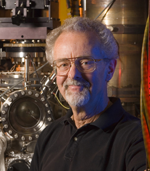
Earl Ward Plummer was an American physicist. His main contributions were in surface physics of metals. Plummer was a professor of physics at Louisiana State University and the University of Pennsylvania prior to that.
In solid-state physics, a metal–semiconductor (M–S) junction is a type of electrical junction in which a metal comes in close contact with a semiconductor material. It is the oldest practical semiconductor device. M–S junctions can either be rectifying or non-rectifying. The rectifying metal–semiconductor junction forms a Schottky barrier, making a device known as a Schottky diode, while the non-rectifying junction is called an ohmic contact.

A topological insulator is a material whose interior behaves as an electrical insulator while its surface behaves as an electrical conductor, meaning that electrons can only move along the surface of the material.
Flow focusing in fluid dynamics is a technology whose aim is the production of drops or bubbles by straightforward hydrodynamic means. The output is a dispersed liquid or gas, frequently in the form of a fine aerosol or an emulsion. No other driving force is required, apart from traditional pumping, a key difference with other comparable technologies, such as electrospray. Both flow focusing and electrospray working in their most extensively used regime produce high quality sprays composed by homogeneous and well-controlled-size droplets. Flow focusing was invented by Prof. Alfonso M. Gañan-Calvo in 1994, patented in 1996, and published for the first time in 1998.
The organic electrochemical transistor (OECT) is an organic electronic device which functions like a transistor. The current flowing through the device is controlled by the exchange of ions between an electrolyte and the OECT channel composed of an organic conductor or semiconductor. The exchange of ions is driven by a voltage applied to the gate electrode which is in ionic contact with the channel through the electrolyte. The migration of ions between the channel and the electrolyte is accompanied by electrochemical redox reactions occurring in the channel material. The electrochemical redox of the channel along with ion migration changes the conductivity of the channel in a process called electrochemical doping. OECTs are being explored for applications in biosensors, bioelectronics and large-area, low-cost electronics. OECTs can also be used as multi-bit memory devices that mimic the synaptic functionalities of the brain. For this reason, OECTs can be also being investigated as elements in neuromorphic computing applications.

Contorted aromatics or more precisely contorted polycyclic aromatic hydrocarbons are polycyclic aromatic hydrocarbons (PAHs) in which the fused aromatic molecules deviate from the usual planarity.

Zhong Lin Wang is a Chinese-American physicist, materials scientist and engineer specialized in nanotechnology, energy science and electronics. He received his PhD from Arizona State University in 1987. He is the Hightower Chair in Materials Science and Engineering and Regents' Professor at the Georgia Institute of Technology, US.
Electroreflectance is the change of reflectivity of a solid due to the influence of an electric field close to, or at the interface of the solid with a liquid. The change in reflectivity is most noticeable at very specific ranges of photon energy, corresponding to the band gaps at critical points of the Brillouin zone.

