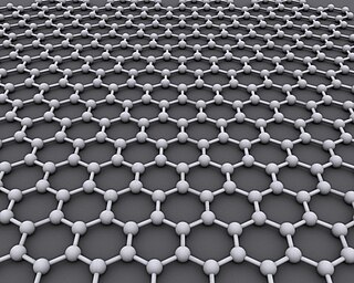
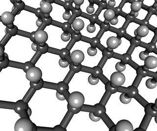
Graphene is an allotrope of carbon consisting of a single layer of atoms arranged in a hexagonal lattice nanostructure. The name is derived from "graphite" and the suffix -ene, reflecting the fact that the graphite allotrope of carbon contains numerous double bonds.

Graphene nanoribbons are strips of graphene with width less than 100 nm. Graphene ribbons were introduced as a theoretical model by Mitsutaka Fujita and coauthors to examine the edge and nanoscale size effect in graphene.

Graphite oxide (GO), formerly called graphitic oxide or graphitic acid, is a compound of carbon, oxygen, and hydrogen in variable ratios, obtained by treating graphite with strong oxidizers and acids for resolving of extra metals. The maximally oxidized bulk product is a yellow solid with C:O ratio between 2.1 and 2.9, that retains the layer structure of graphite but with a much larger and irregular spacing.
Graphane is a two-dimensional polymer of carbon and hydrogen with the formula unit (CH)n where n is large. Partial hydrogenation results in hydrogenated graphene, which was reported by Elias et al in 2009 by a TEM study to be "direct evidence for a new graphene-based derivative". The authors viewed the panorama as "a whole range of new two-dimensional crystals with designed electronic and other properties".
Carbide-derived carbon (CDC), also known as tunable nanoporous carbon, is the common term for carbon materials derived from carbide precursors, such as binary (e.g. SiC, TiC), or ternary carbides, also known as MAX phases (e.g., Ti2AlC, Ti3SiC2). CDCs have also been derived from polymer-derived ceramics such as Si-O-C or Ti-C, and carbonitrides, such as Si-N-C. CDCs can occur in various structures, ranging from amorphous to crystalline carbon, from sp2- to sp3-bonded, and from highly porous to fully dense. Among others, the following carbon structures have been derived from carbide precursors: micro- and mesoporous carbon, amorphous carbon, carbon nanotubes, onion-like carbon, nanocrystalline diamond, graphene, and graphite. Among carbon materials, microporous CDCs exhibit some of the highest reported specific surface areas (up to more than 3000 m2/g). By varying the type of the precursor and the CDC synthesis conditions, microporous and mesoporous structures with controllable average pore size and pore size distributions can be produced. Depending on the precursor and the synthesis conditions, the average pore size control can be applied at sub-Angstrom accuracy. This ability to precisely tune the size and shapes of pores makes CDCs attractive for selective sorption and storage of liquids and gases (e.g., hydrogen, methane, CO2) and the high electric conductivity and electrochemical stability allows these structures to be effectively implemented in electrical energy storage and capacitive water desalinization.

Rodney S. "Rod" Ruoff is an American physical chemist and nanoscience researcher. He is one of the world experts on carbon materials including carbon nanostructures such as fullerenes, nanotubes, graphene, diamond, and has had pioneering discoveries on such materials and others. Ruoff received his B.S. in Chemistry from the University of Texas at Austin (1981) and his Ph.D. in Chemical Physics at the University of Illinois-Urbana (1988). After a Fulbright Fellowship at the MPI fuer Stroemungsforschung in Goettingen, Germany (1989) and postdoctoral work at the IBM T. J. Watson Research Center (1990–91), Ruoff became a staff scientist in the Molecular Physics Laboratory at SRI International (1991–1996). He is currently UNIST Distinguished Professor at the Ulsan National Institute of Science and Technology (UNIST), and the director of the Center for Multidimensional Carbon Materials, an Institute for Basic Science Center located at UNIST.

Fluorographene (or perfluorographane, graphene fluoride) is a fluorocarbon derivative of graphene. It is a two dimensional carbon sheet of sp3 hybridized carbons, with each carbon atom bound to one fluorine. The chemical formula is (CF)n. In comparison, Teflon (polytetrafluoroethylene), -(CF2)n-, consists of carbon "chains" with each carbon bound to two fluorines.
Silicene is a two-dimensional allotrope of silicon, with a hexagonal honeycomb structure similar to that of graphene. Contrary to graphene, silicene is not flat, but has a periodically buckled topology; the coupling between layers in silicene is much stronger than in multilayered graphene; and the oxidized form of silicene, 2D silica, has a very different chemical structure from graphene oxide.
Bilayer graphene is a material consisting of two layers of graphene. One of the first reports of bilayer graphene was in the seminal 2004 Science paper by Geim and colleagues, in which they described devices "which contained just one, two, or three atomic layers"
Germanane is a single-layer crystal composed of germanium with one hydrogen bonded in the z-direction for each atom, in contrast to germanene which contains no hydrogen. In material science, great interest is shown in related single layered materials, such as graphene, composed of carbon, and silicene, composed of silicon. Such materials represent a new generation of semiconductors with potential applications in computer chips and solar cells. Germanane's structure is similar to graphane, and therefore graphene. Bulk germanium does not adopt this structure. Germanane has been produced in a two-step route starting with calcium germanide. From this material, the calcium is removed by de-intercalation with HCl to give a layered solid with the empirical formula GeH. The Ca sites in Zintl phase CaGe2 interchange with the H atoms in the HCl solution, which leaves GeH and CaCl2.
A nanosheet is a two-dimensional nanostructure with thickness in a scale ranging from 1 to 100 nm.
Potential graphene applications include lightweight, thin, and flexible electric/photonics circuits, solar cells, and various medical, chemical and industrial processes enhanced or enabled by the use of new graphene materials.
In materials science, the term single-layer materials or 2D materials refers to crystalline solids consisting of a single layer of atoms. These materials are promising for some applications but remain the focus of research. Single-layer materials derived from single elements generally carry the -ene suffix in their names, e.g. graphene. Single-layer materials that are compounds of two or more elements have -ane or -ide suffixes. 2D materials can generally be categorized as either 2D allotropes of various elements or as compounds.

Germanene is a material made up of a single layer of germanium atoms. The material is created in a process similar to that of silicene and graphene, in which high vacuum and high temperature are used to deposit a layer of germanium atoms on a substrate. High-quality thin films of germanene have revealed unusual two-dimensional structures with novel electronic properties suitable for semiconductor device applications and materials science research.

Penta-graphene is a hypothetical carbon allotrope composed entirely of carbon pentagons and resembling the Cairo pentagonal tiling. Penta-graphene was proposed in 2014 on the basis of analyses and simulations. Further calculations predicted that it is unstable in its pure form, but can be stabilized by hydrogenation. Due to its atomic configuration, penta-graphene has an unusually negative Poisson’s ratio and very high ideal strength believed to exceed that of a similar material, graphene.
A two-dimensional semiconductor is a type of natural semiconductor with thicknesses on the atomic scale. Geim and Novoselov et al. initiated the field in 2004 when they reported a new semiconducting material graphene, a flat monolayer of carbon atoms arranged in a 2D honeycomb lattice. A 2D monolayer semiconductor is significant because it exhibits stronger piezoelectric coupling than traditionally employed bulk forms. This coupling could enable applications. One research focus is on designing nanoelectronic components by the use of graphene as electrical conductor, hexagonal boron nitride as electrical insulator, and a transition metal dichalcogenide as semiconductor.
A rapidly increasing list of graphene production techniques have been developed to enable graphene's use in commercial applications.

Boron nitride nanosheet is a two-dimensional crystalline form of the hexagonal boron nitride (h-BN), which has a thickness of one to few atomic layers. It is similar in geometry as well as physical and thermal properties to its all-carbon analog graphene, but has very different chemical and electronic properties – contrary to the black and highly conducting graphene, BN nanosheets are electrical insulators with a band gap of ~5.9 eV, and therefore appear white in color.
Graphene is a 2D nanosheet with atomic thin thickness in terms of 0.34 nm. Due to the ultrathin thickness, graphene showed many properties that are quite different from their bulk graphite counterparts. The most prominent advantages are known to be their high electron mobility and high mechanical strengths. Thus, it exhibits potential for applications in optics and electronics especially for the development of wearable devices as flexible substrates. More importantly, the optical absorption rate of graphene is 2.3% in the visible and near-infrared region. This broadband absorption characteristic also attracted great attention of the research community to exploit the graphene-based photodetectors/modulators.
Graphene is the only form of carbon in which every atom is available for chemical reaction from two sides. Atoms at the edges of a graphene sheet have special chemical reactivity. Graphene has the highest ratio of edge atoms of any allotrope. Defects within a sheet increase its chemical reactivity. The onset temperature of reaction between the basal plane of single-layer graphene and oxygen gas is below 260 °C (530 K). Graphene combusts at 350 °C (620 K). Graphene is commonly modified with oxygen- and nitrogen-containing functional groups and analyzed by infrared spectroscopy and X-ray photoelectron spectroscopy. However, determination of structures of graphene with oxygen- and nitrogen- functional groups requires the structures to be well controlled.


