Related Research Articles

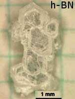
Boron nitride is a thermally and chemically resistant refractory compound of boron and nitrogen with the chemical formula BN. It exists in various crystalline forms that are isoelectronic to a similarly structured carbon lattice. The hexagonal form corresponding to graphite is the most stable and soft among BN polymorphs, and is therefore used as a lubricant and an additive to cosmetic products. The cubic variety analogous to diamond is called c-BN; it is softer than diamond, but its thermal and chemical stability is superior. The rare wurtzite BN modification is similar to lonsdaleite but slightly softer than the cubic form.

Chemical vapor deposition (CVD) is a vacuum deposition method used to produce high-quality, and high-performance, solid materials. The process is often used in the semiconductor industry to produce thin films.

Tungsten(VI) fluoride, also known as tungsten hexafluoride, is an inorganic compound with the formula WF6. It is a toxic, corrosive, colorless gas, with a density of about 13 kg/m3 (22 lb/cu yd). It is the only known gaseous transition metal compound and the densest known gas under standard ambient temperature and pressure. WF6 is commonly used by the semiconductor industry to form tungsten films, through the process of chemical vapor deposition. This layer is used in a low-resistivity metallic "interconnect". It is one of seventeen known binary hexafluorides.
A thin film is a layer of materials ranging from fractions of a nanometer (monolayer) to several micrometers in thickness. The controlled synthesis of materials as thin films is a fundamental step in many applications. A familiar example is the household mirror, which typically has a thin metal coating on the back of a sheet of glass to form a reflective interface. The process of silvering was once commonly used to produce mirrors, while more recently the metal layer is deposited using techniques such as sputtering. Advances in thin film deposition techniques during the 20th century have enabled a wide range of technological breakthroughs in areas such as magnetic recording media, electronic semiconductor devices, integrated passive devices, light-emitting diodes, optical coatings, hard coatings on cutting tools, and for both energy generation and storage. It is also being applied to pharmaceuticals, via thin-film drug delivery. A stack of thin films is called a multilayer.
Plating is a finishing process in which a metal is deposited on a surface. Plating has been done for hundreds of years; it is also critical for modern technology. Plating is used to decorate objects, for corrosion inhibition, to improve solderability, to harden, to improve wearability, to reduce friction, to improve paint adhesion, to alter conductivity, to improve IR reflectivity, for radiation shielding, and for other purposes. Jewelry typically uses plating to give a silver or gold finish.
Atomic layer deposition (ALD) is a thin-film deposition technique based on the sequential use of a gas-phase chemical process; it is a subclass of chemical vapour deposition. The majority of ALD reactions use two chemicals called precursors. These precursors react with the surface of a material one at a time in a sequential, self-limiting, manner. A thin film is slowly deposited through repeated exposure to separate precursors. ALD is a key process in fabricating semiconductor devices, and part of the set of tools for synthesizing nanomaterials.

Parylene is the common name of a polymer whose backbone consists of para-benzenediyl rings −C
6H
4− connected by 1,2-ethanediyl bridges −CH
2−CH
2−. It can be obtained by polymerization of para-xylyleneH
2C=C
6H
4=CH
2.
Electron-beam physical vapor deposition, or EBPVD, is a form of physical vapor deposition in which a target anode is bombarded with an electron beam given off by a charged tungsten filament under high vacuum. The electron beam causes atoms from the target to transform into the gaseous phase. These atoms then precipitate into solid form, coating everything in the vacuum chamber with a thin layer of the anode material.

Vacuum deposition is a group of processes used to deposit layers of material atom-by-atom or molecule-by-molecule on a solid surface. These processes operate at pressures well below atmospheric pressure. The deposited layers can range from a thickness of one atom up to millimeters, forming freestanding structures. Multiple layers of different materials can be used, for example to form optical coatings. The process can be qualified based on the vapor source; physical vapor deposition uses a liquid or solid source and chemical vapor deposition uses a chemical vapor.

Physical vapor deposition (PVD), sometimes called physical vapor transport (PVT), describes a variety of vacuum deposition methods which can be used to produce thin films and coatings on substrates including metals, ceramics, glass, and polymers. PVD is characterized by a process in which the material transitions from a condensed phase to a vapor phase and then back to a thin film condensed phase. The most common PVD processes are sputtering and evaporation. PVD is used in the manufacturing of items which require thin films for optical, mechanical, electrical, acoustic or chemical functions. Examples include semiconductor devices such as thin-film solar cells, microelectromechanical devices such as thin film bulk acoustic resonator, aluminized PET film for food packaging and balloons, and titanium nitride coated cutting tools for metalworking. Besides PVD tools for fabrication, special smaller tools used mainly for scientific purposes have been developed.

Thermal spraying techniques are coating processes in which melted materials are sprayed onto a surface. The "feedstock" is heated by electrical or chemical means.

Thermal barrier coatings (TBCs) are advanced materials systems usually applied to metallic surfaces on parts operating at elevated temperatures, such as gas turbine combustors and turbines, and in automotive exhaust heat management. These 100 μm to 2 mm thick coatings of thermally insulating materials serve to insulate components from large and prolonged heat loads and can sustain an appreciable temperature difference between the load-bearing alloys and the coating surface. In doing so, these coatings can allow for higher operating temperatures while limiting the thermal exposure of structural components, extending part life by reducing oxidation and thermal fatigue. In conjunction with active film cooling, TBCs permit working fluid temperatures higher than the melting point of the metal airfoil in some turbine applications. Due to increasing demand for more efficient engines running at higher temperatures with better durability/lifetime and thinner coatings to reduce parasitic mass for rotating/moving components, there is significant motivation to develop new and advanced TBCs. The material requirements of TBCs are similar to those of heat shields, although in the latter application emissivity tends to be of greater importance.

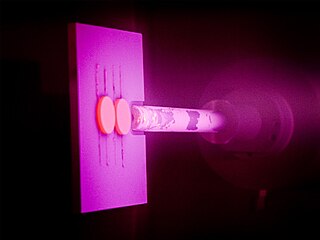
Plasma-enhanced chemical vapor deposition (PECVD) is a chemical vapor deposition process used to deposit thin films from a gas state (vapor) to a solid state on a substrate. Chemical reactions are involved in the process, which occur after creation of a plasma of the reacting gases. The plasma is generally created by radio frequency (RF) alternating current (AC) frequency or direct current (DC) discharge between two electrodes, the space between which is filled with the reacting gases.

Sputter deposition is a physical vapor deposition (PVD) method of thin film deposition by the phenomenon of sputtering. This involves ejecting material from a "target" that is a source onto a "substrate" such as a silicon wafer.
Substrate is a term used in materials science and engineering to describe the base material on which processing is conducted. Surfaces have different uses, including producing new film or layers of material and being a base to which another substance is bonded.
Electrostatic spray-assisted vapour deposition (ESAVD) is a technique to deposit both thin and thick layers of a coating onto various substrates. In simple terms chemical precursors are sprayed across an electrostatic field towards a heated substrate, the chemicals undergo a controlled chemical reaction and are deposited on the substrate as the required coating. Electrostatic spraying techniques were developed in the 1950s for the spraying of ionised particles on to charged or heated substrates.

Zirconium diboride (ZrB2) is a highly covalent refractory ceramic material with a hexagonal crystal structure. ZrB2 is an ultra-high temperature ceramic (UHTC) with a melting point of 3246 °C. This along with its relatively low density of ~6.09 g/cm3 (measured density may be higher due to hafnium impurities) and good high temperature strength makes it a candidate for high temperature aerospace applications such as hypersonic flight or rocket propulsion systems. It is an unusual ceramic, having relatively high thermal and electrical conductivities, properties it shares with isostructural titanium diboride and hafnium diboride.

Tantalum(V) ethoxide is a metalorganic compound with formula Ta2(OC2H5)10, often abbreviated as Ta2(OEt)10. It is a colorless solid that dissolves in some organic solvents but hydrolyzes readily. It is used to prepare films of tantalum(V) oxide.
Liquid–feed flame spray pyrolysis (LF-FSP) is one of the most recent iterations in flame spray pyrolysis (FSP) powder production technology. FSP produces metal oxide powders from highly volatile gaseous metal chlorides that are decomposed/oxidized in hydrogen-oxygen flames to form nano-oxide powders. However, products made from FSP's vapor-phase process are limited to Al-, Ti-, Zr-, and Si-based oxides from their metal chlorides. Thus, interest in producing more complex materials required a new methodology, LF-FSP.
Molecular layer deposition (MLD) is a vapour phase thin film deposition technique based on self-limiting surface reactions carried out in a sequential manner. Essentially, MLD resembles the well established technique of atomic layer deposition (ALD) but, whereas ALD is limited to exclusively inorganic coatings, the precursor chemistry in MLD can use small, bifunctional organic molecules as well. This enables, as well as the growth of organic layers in a process similar to polymerization, the linking of both types of building blocks together in a controlled way to build up organic-inorganic hybrid materials.
References
- ↑ Janda, R; Roulet, J. F.; Wulf, M; Tiller, H. J. (2003). "A new adhesive technology for all-ceramics". Dental Materials. 19 (6): 567–73. doi:10.1016/s0109-5641(02)00106-9. PMID 12837406.
- ↑ US 4620988,Garschke, Adelheid; Tiller, Hans-Jürgen& Gobel, Rolandet al.,"Flame hydrolysis coating apparatus particularly for dental prostheses",issued 1986
- ↑ US 5652021,Hunt, Andrew; Cochran, Joe& Carter, William Brent,"Combustion Chemical Vapor Deposition of films and coatings",issued 1997
- ↑ US 6013318,Hunt, Andrew; Cochran, Joe& Carter, William Brent,"Method for the Combustion Chemical Vapor Deposition of films and coatings",issued 2000
- ↑ Kumar, Siva; Kelekanjeri, G.; Carter, W.B.; Hampikian, J.M. (2006). "Deposition of alpha-alumina via combustion chemical vapor deposition". Thin Solid Films. 515 (4): 1905–1911. Bibcode:2006TSF...515.1905K. doi:10.1016/j.tsf.2006.07.033.
- ↑ Hampikian, J.M.; Carter, W.B. (1999). "The combustion chemical vapor deposition of high temperature materials". Materials Science and Engineering A. 267 (1): 7–18. doi:10.1016/S0921-5093(99)00067-2.
- ↑ Valek, B.C.; Hampikian, J.M. (1997). "Silica Thin Films Applied to Ni-20Cr Alloy via Combustion Chemical Vapor Deposition". Surface and Coatings Technology. 94–95: 13–20. doi:10.1016/S0257-8972(97)00469-6.
- ↑ Hendrick, M.R.; Hampikian, J.M.; Carter, W.B. (1998). "Combustion CVD-Applied Alumina Coatings and their Effects on the Oxidation of a Ni-Base Chromia Former". Journal of the Electrochemical Society. 145 (11): 3986–3994. doi:10.1149/1.1838903.
- ↑ Kuhn, S., Linke, R. and Hädrich, T. (2010). "Modification of hot glass surface with alumina by combustion CVD". Surface and Coatings Technology. 205 (7): 2091–2096. doi:10.1016/j.surfcoat.2010.08.096.
{{cite journal}}: CS1 maint: multiple names: authors list (link)