Processor design is the design engineering task of creating a processor, a key component of computer hardware. It is a subfield of computer engineering and electronics engineering (fabrication). The design process involves choosing an instruction set and a certain execution paradigm and results in a microarchitecture, which might be described in e.g. VHDL or Verilog. For microprocessor design, this description is then manufactured employing some of the various semiconductor device fabrication processes, resulting in a die which is bonded onto a chip carrier. This chip carrier is then soldered onto, or inserted into a socket on, a printed circuit board (PCB).
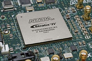
A field-programmable gate array (FPGA) is an integrated circuit designed to be configured by a customer or a designer after manufacturing – hence the term "field-programmable". The FPGA configuration is generally specified using a hardware description language (HDL), similar to that used for an application-specific integrated circuit (ASIC). Circuit diagrams were previously used to specify the configuration, but this is increasingly rare due to the advent of electronic design automation tools.

A programmable logic device (PLD) is an electronic component used to build reconfigurable digital circuits. Unlike integrated circuits (IC) which consist of logic gates and have a fixed function, a PLD has an undefined function at the time of manufacture. Before the PLD can be used in a circuit it must be programmed (reconfigured) by using a specialized program.

A system on a chip is an integrated circuit that integrates all or most components of a computer or other electronic system. These components almost always include a central processing unit (CPU), memory, input/output ports and secondary storage, often alongside other components such as radio modems and a graphics processing unit (GPU) – all on a single substrate or microchip. It may contain digital, analog, mixed-signal, and often radio frequency signal processing functions.

Parallel computing is a type of computation where many calculations or the execution of processes are carried out simultaneously. Large problems can often be divided into smaller ones, which can then be solved at the same time. There are several different forms of parallel computing: bit-level, instruction-level, data, and task parallelism. Parallelism has long been employed in high-performance computing, but has gained broader interest due to the physical constraints preventing frequency scaling. As power consumption by computers has become a concern in recent years, parallel computing has become the dominant paradigm in computer architecture, mainly in the form of multi-core processors.

An application-specific integrated circuit is an integrated circuit (IC) chip customized for a particular use, rather than intended for general-purpose use. For example, a chip designed to run in a digital voice recorder or a high-efficiency bitcoin miner is an ASIC. Application-specific standard product (ASSP) chips are intermediate between ASICs and industry standard integrated circuits like the 7400 series or the 4000 series. ASIC chips are typically fabricated using metal-oxide-semiconductor (MOS) technology, as MOS integrated circuit chips.
Reconfigurable computing is a computer architecture combining some of the flexibility of software with the high performance of hardware by processing with very flexible high speed computing fabrics like field-programmable gate arrays (FPGAs). The principal difference when compared to using ordinary microprocessors is the ability to make substantial changes to the datapath itself in addition to the control flow. On the other hand, the main difference from custom hardware, i.e. application-specific integrated circuits (ASICs) is the possibility to adapt the hardware during runtime by "loading" a new circuit on the reconfigurable fabric.
In computer science, a lookup table is an array that replaces runtime computation with a simpler array indexing operation. The savings in processing time can be significant, because retrieving a value from memory is often faster than carrying out an "expensive" computation or input/output operation. The tables may be precalculated and stored in static program storage, calculated as part of a program's initialization phase (memoization), or even stored in hardware in application-specific platforms. Lookup tables are also used extensively to validate input values by matching against a list of valid items in an array and, in some programming languages, may include pointer functions to process the matching input. FPGAs also make extensive use of reconfigurable, hardware-implemented, lookup tables to provide programmable hardware functionality.

Xilinx, Inc. is an American technology company that is primarily a supplier of programmable logic devices. The company invented the field-programmable gate array (FPGA). It is the semiconductor company that created the first fabless manufacturing model.

A complex programmable logic device (CPLD) is a programmable logic device with complexity between that of PALs and FPGAs, and architectural features of both. The main building block of the CPLD is a macrocell, which contains logic implementing disjunctive normal form expressions and more specialized logic operations.
In computing, hardware acceleration is the use of computer hardware specially made to perform some functions more efficiently than is possible in software running on a general-purpose central processing unit (CPU). Any transformation of data or routine that can be computed, can be calculated purely in software running on a generic CPU, purely in custom-made hardware, or in some mix of both. An operation can be computed faster in application-specific hardware designed or programmed to compute the operation than specified in software and performed on a general-purpose computer processor. Each approach has advantages and disadvantages. The implementation of computing tasks in hardware to decrease latency and increase throughput is known as hardware acceleration.
Stream processing is a computer programming paradigm, equivalent to dataflow programming, event stream processing, and reactive programming, that allows some applications to more easily exploit a limited form of parallel processing. Such applications can use multiple computational units, such as the floating point unit on a graphics processing unit or field-programmable gate arrays (FPGAs), without explicitly managing allocation, synchronization, or communication among those units.
Jingsheng Jason Cong is a Chinese-born American computer scientist, educator, and serial entrepreneur. He received his B.S. degree in computer science from Peking University in 1985, his M.S. and Ph. D. degrees in computer science from the University of Illinois at Urbana-Champaign in 1987 and 1990, respectively. He has been on the faculty in the Computer Science Department at the University of California, Los Angeles (UCLA) since 1990. Currently, he is a Distinguished Chancellor’s Professor and the director of Center for Domain-Specific Computing (CDSC).
This is a glossary of terms used in the field of Reconfigurable computing and reconfigurable computing systems, as opposed to the traditional Von Neumann architecture.
A massively parallel processor array, also known as a multi purpose processor array (MPPA) is a type of integrated circuit which has a massively parallel array of hundreds or thousands of CPUs and RAM memories. These processors pass work to one another through a reconfigurable interconnect of channels. By harnessing a large number of processors working in parallel, an MPPA chip can accomplish more demanding tasks than conventional chips. MPPAs are based on a software parallel programming model for developing high-performance embedded system applications.
Virtex is the flagship family of FPGA products developed by Xilinx. Other current product lines include Kintex (mid-range) and Artix (low-cost), each including configurations and models optimized for different applications. In addition, Xilinx offers the Spartan low-cost series, which continues to be updated and is nearing production utilizing the same underlying architecture and process node as the larger 7-series devices.
Heterogeneous computing refers to systems that use more than one kind of processor or cores. These systems gain performance or energy efficiency not just by adding the same type of processors, but by adding dissimilar coprocessors, usually incorporating specialized processing capabilities to handle particular tasks.
The Xputer is a design for a reconfigurable computer, proposed by computer scientist Reiner Hartenstein. Hartenstein uses various terms to describe the various innovations in the design, including config-ware, flow-ware, morph-ware, and "anti-machine".
In computing, a logic block or configurable logic block (CLB) is a fundamental building block of field-programmable gate array (FPGA) technology. Logic blocks can be configured by the engineer to provide reconfigurable logic gates.
Verilog-to-Routing (VTR) is an open source CAD flow for FPGA devices. VTR's main purpose is to map a given circuit described in Verilog, a Hardware Description Language, on a given FPGA architecture for research and development purposes; the FPGA architecture targeted could be a novel architecture that a researcher wishes to explore, or it could be an existing commercial FPGA whose architecture has been captured in the VTR input format. The VTR project has many contributors, with lead collaborating universities being the University of Toronto, the University of New Brunswick, and the University of California, Berkeley. Additional contributors include Google, The University of Utah, Princeton University, Altera, Intel, Texas Instruments, and MIT Lincoln Lab.