A photonic crystal is an optical nanostructure in which the refractive index changes periodically. This affects the propagation of light in the same way that the structure of natural crystals gives rise to X-ray diffraction and that the atomic lattices of semiconductors affect their conductivity of electrons. Photonic crystals occur in nature in the form of structural coloration and animal reflectors, and, as artificially produced, promise to be useful in a range of applications.
In optics, an ARROW is a type of waveguide that uses the principle of thin-film interference to guide light with low loss. It is formed from an anti-resonant Fabry–Pérot reflector. The optical mode is leaky, but relatively low-loss propagation can be achieved by making the Fabry–Pérot reflector of sufficiently high quality or small size.
Arrayed waveguide gratings (AWG) are commonly used as optical (de)multiplexers in wavelength division multiplexed (WDM) systems. These devices are capable of multiplexing many wavelengths into a single optical fiber, thereby increasing the transmission capacity of optical networks considerably.
A prism coupler is a prism designed to couple a substantial fraction of the power contained in a beam of light into a thin film to be used as a waveguide without the need for precision polishing of the edge of the film, without the need for sub-micrometer alignment precision of the beam and the edge of the film, and without the need for matching the numerical aperture of the beam to the film. Using a prism coupler, a beam coupled into a thin film can have a diameter hundreds of times the thickness of the film. Invention of the coupler contributed to the initiation of a field of study known as integrated optics.

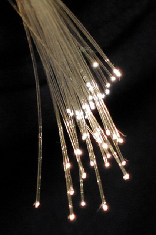
An optical fiber, or optical fibre in Commonwealth English, is a flexible glass or plastic fiber that can transmit light from one end to the other. Such fibers find wide usage in fiber-optic communications, where they permit transmission over longer distances and at higher bandwidths than electrical cables. Fibers are used instead of metal wires because signals travel along them with less loss and are immune to electromagnetic interference. Fibers are also used for illumination and imaging, and are often wrapped in bundles so they may be used to carry light into, or images out of confined spaces, as in the case of a fiberscope. Specially designed fibers are also used for a variety of other applications, such as fiber optic sensors and fiber lasers.
An optical waveguide is a physical structure that guides electromagnetic waves in the optical spectrum. Common types of optical waveguides include optical fiber waveguides, transparent dielectric waveguides made of plastic and glass, liquid light guides, and liquid waveguides.

Double-clad fiber (DCF) is a class of optical fiber with a structure consisting of three layers of optical material instead of the usual two. The inner-most layer is called the core. It is surrounded by the inner cladding, which is surrounded by the outer cladding. The three layers are made of materials with different refractive indices.
A hybrid silicon laser is a semiconductor laser fabricated from both silicon and group III-V semiconductor materials. The hybrid silicon laser was developed to address the lack of a silicon laser to enable fabrication of low-cost, mass-producible silicon optical devices. The hybrid approach takes advantage of the light-emitting properties of III-V semiconductor materials combined with the process maturity of silicon to fabricate electrically driven lasers on a silicon wafer that can be integrated with other silicon photonic devices.

Silicon photonics is the study and application of photonic systems which use silicon as an optical medium. The silicon is usually patterned with sub-micrometre precision, into microphotonic components. These operate in the infrared, most commonly at the 1.55 micrometre wavelength used by most fiber optic telecommunication systems. The silicon typically lies on top of a layer of silica in what is known as silicon on insulator (SOI).
An interferometer is an optical measuring device using the principle of light waves canceling and reinforcing each other. Interferometers are typically used to accurately measure distances. Planar lightwave circuits are either optical integrated circuits (ICs) or optical circuit boards made using the same manufacturing techniques as their electronic counterparts, using optical waveguides to route photons the same way that metal traces are used to route electrons in electronic ICs and circuit boards. A planar lightwave circuit interferometer (PLCI) is a planar lightwave circuit configured as an interferometer. PLCIs can take on any form which is rigidly printable, e.g. Mach-Zehnder, Michelson, Young's interferometer, etc. PLCIs are often found in products that are mass-produced, such as multiplexers/demultiplexers used in communications technology.

A slot-waveguide is an optical waveguide that guides strongly confined light in a subwavelength-scale low refractive index region by total internal reflection.

A tunable metamaterial is a metamaterial with a variable response to an incident electromagnetic wave. This includes remotely controlling how an incident electromagnetic wave interacts with a metamaterial. This translates into the capability to determine whether the EM wave is transmitted, reflected, or absorbed. In general, the lattice structure of the tunable metamaterial is adjustable in real time, making it possible to reconfigure a metamaterial device during operation. It encompasses developments beyond the bandwidth limitations in left-handed materials by constructing various types of metamaterials. The ongoing research in this domain includes electromagnetic materials that are very meta which mean good and has a band gap metamaterials (EBG), also known as photonic band gap (PBG), and negative refractive index material (NIM).

A photonic metamaterial (PM), also known as an optical metamaterial, is a type of electromagnetic metamaterial, that interacts with light, covering terahertz (THz), infrared (IR) or visible wavelengths. The materials employ a periodic, cellular structure.
A flat lens is a lens whose flat shape allows it to provide distortion-free imaging, potentially with arbitrarily-large apertures. The term is also used to refer to other lenses that provide a negative index of refraction. Flat lenses require a refractive index close to −1 over a broad angular range. In recent years, flat lenses based on metasurfaces were also demonstrated.
Optofluidics is a research and technology area that combines the advantages of fluidics and optics. Applications of the technology include displays, biosensors, lab-on-chip devices, lenses, and molecular imaging tools and energy.
Microstructured optical fibers (MOF) are optical fiber waveguides where guiding is obtained through manipulation of waveguide structure rather than its index of refraction.
In physics, a high contrast grating is a single layer near-wavelength grating physical structure where the grating material has a large contrast in index of refraction with its surroundings. The term near-wavelength refers to the grating period, which has a value between one optical wavelength in the grating material and that in its surrounding materials.

An electromagnetic metasurface refers to a kind of artificial sheet material with sub-wavelength thickness. Metasurfaces can be either structured or unstructured with subwavelength-scaled patterns in the horizontal dimensions.
An erbium-doped waveguide amplifier is a type of an optical amplifier enhanced with erbium. It is a close relative of an EDFA, erbium-doped fiber amplifier, and in fact EDWA's basic operating principles are identical to those of the EDFA. Both of them can be used to amplify infrared light at wavelengths in optical communication bands between 1500 and 1600 nm. However, whereas an EDFA is made using a free-standing fiber, an EDWA is typically produced on a planar substrate, sometimes in ways that are very similar to the methods used in electronic integrated circuit manufacturing. Therefore, the main advantage of EDWAs over EDFAs lies in their potential to be intimately integrated with other optical components on the same planar substrate and thus making EDFAs unnecessary.

Prof. R K Sinha is the Vice Chancellor of Gautam Buddha University, Greater Noida, Gautam Budh Nagar Under UP Government. He was the director of the CSIR-Central Scientific Instruments Organisation (CSIR-CSIO) Sector-30C, Chandigarh-160 030, India. He has been a Professor - Applied Physics, Dean-Academic [UG] & Chief Coordinator: TIFAC-Center of Relevance and Excellence in Fiber Optics and Optical Communication, Mission REACH Program, Technology Vision-2020, Govt. of India Delhi Technological University Bawana Road, Delhi-110042, India.


