Related Research Articles

A central processing unit (CPU), also called a central processor, main processor, or just processor, is the most important processor in a given computer. Its electronic circuitry executes instructions of a computer program, such as arithmetic, logic, controlling, and input/output (I/O) operations. This role contrasts with that of external components, such as main memory and I/O circuitry, and specialized coprocessors such as graphics processing units (GPUs).
Processor design is a subfield of computer science and computer engineering (fabrication) that deals with creating a processor, a key component of computer hardware.

Double Data Rate Synchronous Dynamic Random-Access Memory is a double data rate (DDR) synchronous dynamic random-access memory (SDRAM) class of memory integrated circuits used in computers. DDR SDRAM, also retroactively called DDR1 SDRAM, has been superseded by DDR2 SDRAM, DDR3 SDRAM, DDR4 SDRAM and DDR5 SDRAM. None of its successors are forward or backward compatible with DDR1 SDRAM, meaning DDR2, DDR3, DDR4 and DDR5 memory modules will not work on DDR1-equipped motherboards, and vice versa.
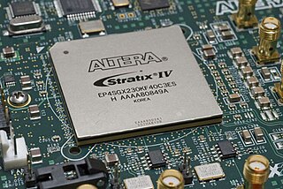
A field-programmable gate array (FPGA) is a type of configurable integrated circuit that can be repeatedly programmed after manufacturing. FPGAs are a subset of logic devices referred to as programmable logic devices (PLDs). They consist of an array of programmable logic blocks with a connecting grid, that can be configured "in the field" to interconnect with other logic blocks to perform various digital functions. FPGAs are often used in limited (low) quantity production of custom-made products, and in research and development, where the higher cost of individual FPGAs is not as important, and where creating and manufacturing a custom circuit wouldn't be feasible. Other applications for FPGAs include the telecommunications, automotive, aerospace, and industrial sectors, which benefit from their flexibility, high signal processing speed, and parallel processing abilities.
In computer engineering, a hardware description language (HDL) is a specialized computer language used to describe the structure and behavior of electronic circuits, most commonly to design ASICs and program FPGAs.

Dynamic random-access memory is a type of random-access semiconductor memory that stores each bit of data in a memory cell, usually consisting of a tiny capacitor and a transistor, both typically based on metal–oxide–semiconductor (MOS) technology. While most DRAM memory cell designs use a capacitor and transistor, some only use two transistors. In the designs where a capacitor is used, the capacitor can either be charged or discharged; these two states are taken to represent the two values of a bit, conventionally called 0 and 1. The electric charge on the capacitors gradually leaks away; without intervention the data on the capacitor would soon be lost. To prevent this, DRAM requires an external memory refresh circuit which periodically rewrites the data in the capacitors, restoring them to their original charge. This refresh process is the defining characteristic of dynamic random-access memory, in contrast to static random-access memory (SRAM) which does not require data to be refreshed. Unlike flash memory, DRAM is volatile memory, since it loses its data quickly when power is removed. However, DRAM does exhibit limited data remanence.

An application-specific integrated circuit is an integrated circuit (IC) chip customized for a particular use, rather than intended for general-purpose use, such as a chip designed to run in a digital voice recorder or a high-efficiency video codec. Application-specific standard product chips are intermediate between ASICs and industry standard integrated circuits like the 7400 series or the 4000 series. ASIC chips are typically fabricated using metal–oxide–semiconductor (MOS) technology, as MOS integrated circuit chips.

In computing, overclocking is the practice of increasing the clock rate of a computer to exceed that certified by the manufacturer. Commonly, operating voltage is also increased to maintain a component's operational stability at accelerated speeds. Semiconductor devices operated at higher frequencies and voltages increase power consumption and heat. An overclocked device may be unreliable or fail completely if the additional heat load is not removed or power delivery components cannot meet increased power demands. Many device warranties state that overclocking or over-specification voids any warranty, but some manufacturers allow overclocking as long as it is done (relatively) safely.

In electronics and especially synchronous digital circuits, a clock signal is an electronic logic signal which oscillates between a high and a low state at a constant frequency and is used like a metronome to synchronize actions of digital circuits. In a synchronous logic circuit, the most common type of digital circuit, the clock signal is applied to all storage devices, flip-flops and latches, and causes them all to change state simultaneously, preventing race conditions.
In electronic design automation, a design rule is a geometric constraint imposed on circuit board, semiconductor device, and integrated circuit (IC) designers to ensure their designs function properly, reliably, and can be produced with acceptable yield. Design rules for production are developed by process engineers based on the capability of their processes to realize design intent. Electronic design automation is used extensively to ensure that designers do not violate design rules; a process called design rule checking (DRC). DRC is a major step during physical verification signoff on the design, which also involves LVS checks, XOR checks, ERC, and antenna checks. The importance of design rules and DRC is greatest for ICs, which have micro- or nano-scale geometries; for advanced processes, some fabs also insist upon the use of more restricted rules to improve yield.
Static timing analysis (STA) is a simulation method of computing the expected timing of a synchronous digital circuit without requiring a simulation of the full circuit.

Integrated circuit design, semiconductor design, chip design or IC design, is a sub-field of electronics engineering, encompassing the particular logic and circuit design techniques required to design integrated circuits, or ICs. ICs consist of miniaturized electronic components built into an electrical network on a monolithic semiconductor substrate by photolithography.
Logic simulation is the use of simulation software to predict the behavior of digital circuits and hardware description languages. Simulation can be performed at varying degrees of physical abstraction, such as at the transistor level, gate level, register-transfer level (RTL), electronic system-level (ESL), or behavioral level.

In integrated circuit design, hardware emulation is the process of imitating the behavior of one or more pieces of hardware with another piece of hardware, typically a special purpose emulation system. The emulation model is usually based on a hardware description language source code, which is compiled into the format used by emulation system. The goal is normally debugging and functional verification of the system being designed. Often an emulator is fast enough to be plugged into a working target system in place of a yet-to-be-built chip, so the whole system can be debugged with live data. This is a specific case of in-circuit emulation.
Design Closure is a part of the digital electronic design automation workflow by which an integrated circuit design is modified from its initial description to meet a growing list of design constraints and objectives.
In computing, computer performance is the amount of useful work accomplished by a computer system. Outside of specific contexts, computer performance is estimated in terms of accuracy, efficiency and speed of executing computer program instructions. When it comes to high computer performance, one or more of the following factors might be involved:

In integrated circuit design, physical design is a step in the standard design cycle which follows after the circuit design. At this step, circuit representations of the components of the design are converted into geometric representations of shapes which, when manufactured in the corresponding layers of materials, will ensure the required functioning of the components. This geometric representation is called integrated circuit layout. This step is usually split into several sub-steps, which include both design and verification and validation of the layout.
Low-power electronics are electronics, such as notebook processors, that have been designed to use less electrical power than usual, often at some expense. In the case of notebook processors, this expense is processing power; notebook processors usually consume less power than their desktop counterparts, at the expense of lower processing power.
In the automated design of integrated circuits, signoff checks is the collective name given to a series of verification steps that the design must pass before it can be taped out. This implies an iterative process involving incremental fixes across the board using one or more check types, and then retesting the design. There are two types of sign-off's: front-end sign-off and back-end sign-off. After back-end sign-off, the chip goes to fabrication. After listing out all the features in the specification, the verification engineer will write coverage for those features to identify bugs, and send back the RTL design to the designer. Bugs, or defects, can include issues like missing features, errors in design, etc. When the coverage reaches a maximum percentage then the verification team will sign it off. By using a methodology like UVM, OVM, or VMM, the verification team develops a reusable environment. Nowadays, UVM is more popular than others.
Xilinx ISE is a discontinued software tool from Xilinx for synthesis and analysis of HDL designs, which primarily targets development of embedded firmware for Xilinx FPGA and CPLD integrated circuit (IC) product families. It was succeeded by Xilinx Vivado. Use of the last released edition from October 2013 continues for in-system programming of legacy hardware designs containing older FPGAs and CPLDs otherwise orphaned by the replacement design tool, Vivado Design Suite.