Related Research Articles

Condensed matter physics is the field of physics that deals with the macroscopic and microscopic physical properties of matter, especially the solid and liquid phases, that arise from electromagnetic forces between atoms and electrons. More generally, the subject deals with condensed phases of matter: systems of many constituents with strong interactions among them. More exotic condensed phases include the superconducting phase exhibited by certain materials at extremely low cryogenic temperatures, the ferromagnetic and antiferromagnetic phases of spins on crystal lattices of atoms, the Bose–Einstein condensates found in ultracold atomic systems, and liquid crystals. Condensed matter physicists seek to understand the behavior of these phases by experiments to measure various material properties, and by applying the physical laws of quantum mechanics, electromagnetism, statistical mechanics, and other physics theories to develop mathematical models and predict the properties of extremely large groups of atoms.
A semiconductor is a material that is between the conductor and insulator in ability to conduct electrical current. In many cases their conducting properties may be altered in useful ways by introducing impurities ("doping") into the crystal structure. When two differently doped regions exist in the same crystal, a semiconductor junction is created. The behavior of charge carriers, which include electrons, ions, and electron holes, at these junctions is the basis of diodes, transistors, and most modern electronics. Some examples of semiconductors are silicon, germanium, gallium arsenide, and elements near the so-called "metalloid staircase" on the periodic table. After silicon, gallium arsenide is the second-most common semiconductor and is used in laser diodes, solar cells, microwave-frequency integrated circuits, and others. Silicon is a critical element for fabricating most electronic circuits.

An exciton is a bound state of an electron and an electron hole which are attracted to each other by the electrostatic Coulomb force resulting from their opposite charges. It is an electrically neutral quasiparticle regarded as an elementary excitation primarily in condensed matter, such as insulators, semiconductors, some metals, and in some liquids. It transports energy without transporting net electric charge.
Solid-state physics is the study of rigid matter, or solids, through methods such as solid-state chemistry, quantum mechanics, crystallography, electromagnetism, and metallurgy. It is the largest branch of condensed matter physics. Solid-state physics studies how the large-scale properties of solid materials result from their atomic-scale properties. Thus, solid-state physics forms a theoretical basis of materials science. Along with solid-state chemistry, it also has direct applications in the technology of transistors and semiconductors.
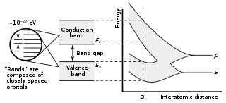
In solid-state physics and solid-state chemistry, a band gap, also called a bandgap or energy gap, is an energy range in a solid where no electronic states exist. In graphs of the electronic band structure of solids, the band gap refers to the energy difference between the top of the valence band and the bottom of the conduction band in insulators and semiconductors. It is the energy required to promote an electron from the valence band to the conduction band. The resulting conduction-band electron are free to move within the crystal lattice and serve as charge carriers to conduct electric current. It is closely related to the HOMO/LUMO gap in chemistry. If the valence band is completely full and the conduction band is completely empty, then electrons cannot move within the solid because there are no available states. If the electrons are not free to move within the crystal lattice, then there is no generated current due to no net charge carrier mobility. However, if some electrons transfer from the valence band to the conduction band, then current can flow. Therefore, the band gap is a major factor determining the electrical conductivity of a solid. Substances having large band gaps are generally insulators, those with small band gaps are semiconductors, and conductors either have very small band gaps or none, because the valence and conduction bands overlap to form a continuous band.

In physics, chemistry, and electronic engineering, an electron hole is a quasiparticle denoting the lack of an electron at a position where one could exist in an atom or atomic lattice. Since in a normal atom or crystal lattice the negative charge of the electrons is balanced by the positive charge of the atomic nuclei, the absence of an electron leaves a net positive charge at the hole's location.
In solid state physics, a particle's effective mass is the mass that it seems to have when responding to forces, or the mass that it seems to have when interacting with other identical particles in a thermal distribution. One of the results from the band theory of solids is that the movement of particles in a periodic potential, over long distances larger than the lattice spacing, can be very different from their motion in a vacuum. The effective mass is a quantity that is used to simplify band structures by modeling the behavior of a free particle with that mass. For some purposes and some materials, the effective mass can be considered to be a simple constant of a material. In general, however, the value of effective mass depends on the purpose for which it is used, and can vary depending on a number of factors.
The electron affinity (Eea) of an atom or molecule is defined as the amount of energy released when an electron attaches to a neutral atom or molecule in the gaseous state to form an anion.
In solid-state physics, the electronic band structure of a solid describes the range of energy levels that electrons may have within it, as well as the ranges of energy that they may not have.

A semimetal is a material with a small energy overlap between the bottom of the conduction band and the top of the valence band, but they do not overlap in momentum space. According to electronic band theory, solids can be classified as insulators, semiconductors, semimetals, or metals. In insulators and semiconductors the filled valence band is separated from an empty conduction band by a band gap. For insulators, the magnitude of the band gap is larger than that of a semiconductor. Because of the slight overlap between the conduction and valence bands, semimetals have no band gap and a small density of states at the Fermi level. A metal, by contrast, has an appreciable density of states at the Fermi level because the conduction band is partially filled.
A superlattice is a periodic structure of layers of two materials. Typically, the thickness of one layer is several nanometers. It can also refer to a lower-dimensional structure such as an array of quantum dots or quantum wells.
Per-Olov Löwdin was a Swedish physicist, professor at the University of Uppsala from 1960 to 1983, and in parallel at the University of Florida until 1993.
Ab initio quantum chemistry methods are computational chemistry methods based on quantum chemistry. The term ab initio was first used in quantum chemistry by Robert Parr and coworkers, including David Craig in a semiempirical study on the excited states of benzene. The background is described by Parr. Ab initio means "from first principles" or "from the beginning", implying that the only inputs into an ab initio calculation are physical constants. Ab initio quantum chemistry methods attempt to solve the electronic Schrödinger equation given the positions of the nuclei and the number of electrons in order to yield useful information such as electron densities, energies and other properties of the system. The ability to run these calculations has enabled theoretical chemists to solve a range of problems and their importance is highlighted by the awarding of the Nobel prize to John Pople and Walter Kohn.
Marvin Lou Cohen is an American–Canadian theoretical physicist. He is a physics professor at the University of California, Berkeley. Cohen is a leading expert in the field of condensed matter physics. He is widely known for his seminal work on the electronic structure of solids.
In solid-state physics, a metal–semiconductor (M–S) junction is a type of electrical junction in which a metal comes in close contact with a semiconductor material. It is the oldest type of practical semiconductor device. M–S junctions can either be rectifying or non-rectifying. The rectifying metal–semiconductor junction forms a Schottky barrier, making a device known as a Schottky diode, while the non-rectifying junction is called an ohmic contact.
In solid-state physics, the k·p perturbation theory is an approximated semi-empirical approach for calculating the band structure and optical properties of crystalline solids. It is pronounced "k dot p", and is also called the k·p method. This theory has been applied specifically in the framework of the Luttinger–Kohn model, and of the Kane model.
Reflectance difference spectroscopy(RDS) is a spectroscopic technique which measures the difference in reflectance of two beams of light that are shone in normal incident on a surface with different linear polarizations. It is also known as reflectance anisotropy spectroscopy (RAS).
In solid-state physics, the valence band and conduction band are the bands closest to the Fermi level, and thus determine the electrical conductivity of the solid. In nonmetals, the valence band is the highest range of electron energies in which electrons are normally present at absolute zero temperature, while the conduction band is the lowest range of vacant electronic states. On a graph of the electronic band structure of a semiconducting material, the valence band is located below the Fermi level, while the conduction band is located above it.
Elias Burstein was an American experimental condensed matter physicist whose active career in science spanned seven decades. He is known for his pioneering fundamental research in the optical physics of solids; for writing and editing hundreds of articles and other publications; for bringing together scientists from around the world in international meetings, conferences, and symposia; and for training and mentoring dozens of younger physicists.
References
- ↑ Kane, E. O. (January 1, 1966), Willardson, R. K.; Beer, Albert C. (eds.), "Chapter 3 The k •p Method", Semiconductors and Semimetals, Semiconductors and Semimetals, vol. 1, Elsevier, pp. 75–100, retrieved August 15, 2024
- ↑ "Kane, Pennsylvania". Allegheny National Forest Visitors Bureau. Retrieved August 15, 2024.
- 1 2 "Physics Today Daily Edition Departments".
- ↑ "Obituary of Evan O' Neill Kane". Physics Today. 2013. doi:10.1063/pt.4.2301.
- 1 2 3 "Bradley & Son Funeral Homes".
- ↑ Bowen, Norman R.; Zobell, Albert L.; Jr. "General Thomas L. Kane: the Pioneer". www.churchofjesuschrist.org. Retrieved August 15, 2024.
- ↑ Kane, E. O. (1956). "Energy band structure in p-type germanium and silicon". Journal of Physics and Chemistry of Solids. 1 (1–2): 82–99. Bibcode:1956JPCS....1...82K. doi:10.1016/0022-3697(56)90014-2.
- ↑ EO Kane and AB Kane, "Direct calculation of Wannier Functions; Si valence bands, Physical Review B, 17, 2691 (1978).
- ↑ Kane, E. O. (1957). "Band structure of indium antimonide". Journal of Physics and Chemistry of Solids. 1 (4): 249–261. Bibcode:1957JPCS....1..249K. doi:10.1016/0022-3697(57)90013-6.
- 1 2 3 4 5 6 7 8 9 10 11 Citation statistics retrieved from Google Scholar, 28 February 2017
- ↑ Peter Y. Yu and Manuel Cardona, "Fundamentals of Semiconductors, Physics and Materials Properties, Springer, ISBN 978-3-642-00709-5 (Print) 978-3-642-00710-1 (Online)
- ↑ Lok C. Lew Yan Voon and Morten Willatzen, "The k.p Method" Electronic Properties of Semiconductors, Springer, Springer-Verlag Berlin, Heidelberg, 2009. doi : 10.1007/978-3-540-92872-0
| Authority control databases: Academics |
|---|