Related Research Articles
A charge-coupled device (CCD) is an integrated circuit containing an array of linked, or coupled, capacitors. Under the control of an external circuit, each capacitor can transfer its electric charge to a neighboring capacitor. CCD sensors are a major technology used in digital imaging.

The metal-oxide-semiconductor field-effect transistor is a type of field-effect transistor (FET), most commonly fabricated by the controlled oxidation of silicon. It has an insulated gate, the voltage of which determines the conductivity of the device. This ability to change conductivity with the amount of applied voltage can be used for amplifying or switching electronic signals. A metal-insulator-semiconductor field-effect transistor (MISFET) is a term almost synonymous with MOSFET. Another synonym is IGFET for insulated-gate field-effect transistor.
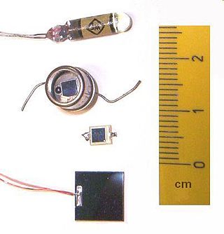
A photodiode is a light-sensitive semiconductor diode. It produces current when it absorbs photons.

Complementary metal–oxide–semiconductor is a type of metal–oxide–semiconductor field-effect transistor (MOSFET) fabrication process that uses complementary and symmetrical pairs of p-type and n-type MOSFETs for logic functions. CMOS technology is used for constructing integrated circuit (IC) chips, including microprocessors, microcontrollers, memory chips, and other digital logic circuits. CMOS technology is also used for analog circuits such as image sensors, data converters, RF circuits, and highly integrated transceivers for many types of communication.
LBCAST is a type of photo sensor which the manufacturer claims is simpler and thus smaller and faster than CMOS sensors. It was developed over ten years by Nikon, in parallel with other manufacturer's development of CMOS, and resulted in shipping product in 2003.
A digital image is an image composed of picture elements, also known as pixels, each with finite, discrete quantities of numeric representation for its intensity or gray level that is an output from its two-dimensional functions fed as input by its spatial coordinates denoted with x, y on the x-axis and y-axis, respectively. Depending on whether the image resolution is fixed, it may be of vector or raster type. By itself, the term "digital image" usually refers to raster images or bitmapped images.

A single-photon avalanche diode (SPAD) is a solid-state photodetector within the same family as photodiodes and avalanche photodiodes (APDs), while also being fundamentally linked with basic diode behaviours. As with photodiodes and APDs, a SPAD is based around a semi-conductor p-n junction that can be illuminated with ionizing radiation such as gamma, x-rays, beta and alpha particles along with a wide portion of the electromagnetic spectrum from ultraviolet (UV) through the visible wavelengths and into the infrared (IR).
In computer engineering, a logic family is one of two related concepts:

Photodetectors, also called photosensors, are sensors of light or other electromagnetic radiation. There are a wide variety of photodetectors which may be classified by mechanism of detection, such as photoelectric or photochemical effects, or by various performance metrics, such as spectral response. Semiconductor-based photodetectors typically use a p–n junction that converts photons into charge. The absorbed photons make electron–hole pairs in the depletion region. Photodiodes and photo transistors are a few examples of photo detectors. Solar cells convert some of the light energy absorbed into electrical energy.

An image sensor or imager is a sensor that detects and conveys information used to form an image. It does so by converting the variable attenuation of light waves into signals, small bursts of current that convey the information. The waves can be light or other electromagnetic radiation. Image sensors are used in electronic imaging devices of both analog and digital types, which include digital cameras, camera modules, camera phones, optical mouse devices, medical imaging equipment, night vision equipment such as thermal imaging devices, radar, sonar, and others. As technology changes, electronic and digital imaging tends to replace chemical and analog imaging.

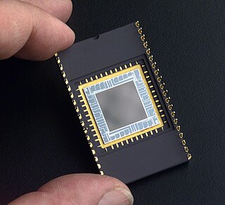
An active-pixel sensor (APS) is an image sensor, which was invented by Peter J.W. Noble in 1968, where each pixel sensor unit cell has a photodetector and one or more active transistors. In a metal–oxide–semiconductor (MOS) active-pixel sensor, MOS field-effect transistors (MOSFETs) are used as amplifiers. There are different types of APS, including the early NMOS APS and the now much more common complementary MOS (CMOS) APS, also known as the CMOS sensor. CMOS sensors are used in digital camera technologies such as cell phone cameras, web cameras, most modern digital pocket cameras, most digital single-lens reflex cameras (DSLRs), mirrorless interchangeable-lens cameras (MILCs), and lensless imaging for cells.

In digital imaging, a color filter array (CFA), or color filter mosaic (CFM), is a mosaic of tiny color filters placed over the pixel sensors of an image sensor to capture color information.

In digital photography, the image sensor format is the shape and size of the image sensor.

Exmor is technology Sony implemented on some of their CMOS image sensors. It performs on-chip analog/digital signal conversion and two-step noise reduction in parallel on each column of the CMOS sensor.
BIONZ is a line of image processors used in Sony digital cameras.
In physics and in electronic engineering, dark current is the relatively small electric current that flows through photosensitive devices such as a photomultiplier tube, photodiode, or charge-coupled device even when no photons enter the device; it consists of the charges generated in the detector when no outside radiation is entering the detector. It is referred to as reverse bias leakage current in non-optical devices and is present in all diodes. Physically, dark current is due to the random generation of electrons and holes within the depletion region of the device.

Paul Suni is a Silicon Valley technologist, engineer, semiconductor device physicist and independent researcher. Since 1984, he has contributed to advancements in semiconductor electronics, photonics, digital imaging sensors and medical devices. In 2007, he dedicated himself to research concerning the scientific and philosophical foundations of technology and wellbeing.

A back-illuminated sensor, also known as backside illumination (BI) sensor, is a type of digital image sensor that uses a novel arrangement of the imaging elements to increase the amount of light captured and thereby improve low-light performance.

The field-effect transistor (FET) is a type of transistor that uses an electric field to control the flow of current in a semiconductor. It comes in two types: junction-gate FET (JFET) and metal-oxide-semiconductor FET (MOSFET). FETs have three terminals: source, gate, and drain. FETs control the flow of current by the application of a voltage to the gate, which in turn alters the conductivity between the drain and source.

There are a variety of technologies available for detecting and recording the images, diffraction patterns, and electron energy loss spectra produced using transmission electron microscopy (TEM).
References
- ↑ Yonemoto, K.; Sumi, H. (2000). "A CMOS image sensor with a simple fixed-pattern-noise-reduction technology and a hole accumulation diode". IEEE Journal of Solid-State Circuits. 35 (12): 2038–2043. Bibcode:2000IJSSC..35.2038Y. doi:10.1109/4.890320. ISSN 0018-9200. S2CID 21187209.
- ↑ "Sony Develops Noise Reduction Technologies to Enhance Image Quality of CMOS Image Sensors". Sony Global. February 8, 2000. Retrieved 2012-12-08.
Press Release