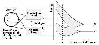
In solid-state physics, a band gap, also called an energy gap, is an energy range in a solid where no electronic states can exist. In graphs of the electronic band structure of solids, the band gap generally refers to the energy difference between the top of the valence band and the bottom of the conduction band in insulators and semiconductors. It is the energy required to promote a valence electron bound to an atom to become a conduction electron, which is free to move within the crystal lattice and serve as a charge carrier to conduct electric current. It is closely related to the HOMO/LUMO gap in chemistry. If the valence band is completely full and the conduction band is completely empty, then electrons cannot move in the solid; however, if some electrons transfer from the valence to the conduction band, then current can flow. Therefore, the band gap is a major factor determining the electrical conductivity of a solid. Substances with large band gaps are generally insulators, those with smaller band gaps are semiconductors, while conductors either have very small band gaps or none, because the valence and conduction bands overlap.

A laser diode, (LD), injection laser diode (ILD), or diode laser is a semiconductor device similar to a light-emitting diode in which a diode pumped directly with electrical current can create lasing conditions at the diode's junction. Laser diodes can directly convert electrical energy into light. Driven by voltage, the doped p-n-transition allows for recombination of an electron with a hole. Due to the drop of the electron from a higher energy level to a lower one, radiation, in the form of an emitted photon is generated. This is spontaneous emission. Stimulated emission can be produced when the process is continued and further generate light with the same phase, coherence and wavelength.

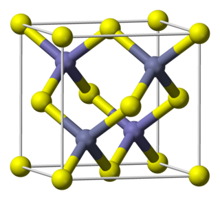
Gallium arsenide (GaAs) is a III-V direct band gap semiconductor with a zinc blende crystal structure.
Wide-bandgap semiconductors are semiconductor materials which have a relatively large band gap compared to conventional semiconductors. Conventional semiconductors like silicon have a bandgap in the range of 1 - 1.5 electronvolt (eV), whereas wide-bandgap materials have bandgaps in the range of 2 - 4 eV. Generally, wide-bandgap semiconductors have electronic properties which fall in between those of conventional semiconductors and insulators.
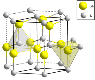
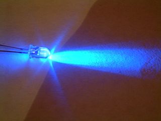
Gallium nitride (GaN) is a binary III/V direct bandgap semiconductor commonly used in blue light-emitting diodes since the 1990s. The compound is a very hard material that has a Wurtzite crystal structure. Its wide band gap of 3.4 eV affords it special properties for applications in optoelectronic, high-power and high-frequency devices. For example, GaN is the substrate which makes violet (405 nm) laser diodes possible, without use of nonlinear optical frequency-doubling.

Zinc oxide is an inorganic compound with the formula ZnO. ZnO is a white powder that is insoluble in water. It is used as an additive in numerous materials and products including cosmetics, food supplements, rubbers, plastics, ceramics, glass, cement, lubricants, paints, ointments, adhesives, sealants, pigments, foods, batteries, ferrites, fire retardants, and first-aid tapes. Although it occurs naturally as the mineral zincite, most zinc oxide is produced synthetically.
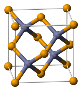
Indium phosphide (InP) is a binary semiconductor composed of indium and phosphorus. It has a face-centered cubic ("zincblende") crystal structure, identical to that of GaAs and most of the III-V semiconductors.
Zinc selenide (ZnSe) is a light-yellow, solid compound comprising zinc (Zn) and selenium (Se). It is an intrinsic semiconductor with a band gap of about 2.70 eV at 25 °C (77 °F). ZnSe rarely occurs in nature, and is found in the mineral that was named after Hans Stille called "stilleite."
Indium gallium arsenide (InGaAs) is a ternary alloy of indium arsenide (InAs) and gallium arsenide (GaAs). Indium and gallium are elements of the periodic table while arsenic is a element. Alloys made of these chemical groups are referred to as "III-V" compounds. InGaAs has properties intermediate between those of GaAs and InAs. InGaAs is a room-temperature semiconductor with applications in electronics and photonics.
Thermophotovoltaic (TPV) energy conversion is a direct conversion process from heat to electricity via photons. A basic thermophotovoltaic system consists of a thermal emitter and a photovoltaic diode cell.
Indium gallium nitride is a semiconductor material made of a mix of gallium nitride (GaN) and indium nitride (InN). It is a ternary group III/group V direct bandgap semiconductor. Its bandgap can be tuned by varying the amount of indium in the alloy. InxGa1−xN has a direct bandgap span from the infrared for InN to the ultraviolet of GaN. The ratio of In/Ga is usually between 0.02/0.98 and 0.3/0.7.
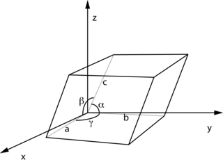
The lattice constant, or lattice parameter, refers to the physical dimension of unit cells in a crystal lattice. Lattices in three dimensions generally have three lattice constants, referred to as a, b, and c. However, in the special case of cubic crystal structures, all of the constants are equal and are referred to as a. Similarly, in hexagonal crystal structures, the a and b constants are equal, and we only refer to the a and c constants. A group of lattice constants could be referred to as lattice parameters. However, the full set of lattice parameters consist of the three lattice constants and the three angles between them.
Indium arsenide, InAs, or indium monoarsenide, is a semiconductor composed of indium and arsenic. It has the appearance of grey cubic crystals with a melting point of 942 °C.

In nanotechnology, nanorods are one morphology of nanoscale objects. Each of their dimensions range from 1–100 nm. They may be synthesized from metals or semiconducting materials. Standard aspect ratios are 3-5. Nanorods are produced by direct chemical synthesis. A combination of ligands act as shape control agents and bond to different facets of the nanorod with different strengths. This allows different faces of the nanorod to grow at different rates, producing an elongated object.
Zinc telluride is a binary chemical compound with the formula ZnTe. This solid is a semiconductor material with a direct band gap of 2.26 eV. It is usually a p-type semiconductor. Its crystal structure is cubic, like that for sphalerite and diamond.
Aluminium gallium indium phosphide is a semiconductor material that provides a platform for the development of novel multi-junction photovoltaics and optoelectronic devices, as it spans a direct bandgap from deep ultraviolet to infrared.

Transparent conducting films (TCFs) are thin films of optically transparent and electrically conductive material. They are an important component in a number of electronic devices including liquid-crystal displays, OLEDs, touchscreens and photovoltaics. While indium tin oxide (ITO) is the most widely used, alternatives include wider-spectrum transparent conductive oxides (TCOs), conductive polymers, metal grids and random metallic networks, carbon nanotubes (CNT), graphene, nanowire meshes and ultra thin metal films.
Non linear piezoelectric effects in polar semiconductors are the manifestation that the strain induced piezoelectric polarization depends not just on the product of the first order piezoelectric coefficients times the strain tensor components but also on the product of the second order piezoelectric coefficients times products of the strain tensor components. The idea was put forward for zincblende GaAs and InAs semiconductors since 2006, and then extended to all commonly used wurtzite and zincblende semiconductors. Given the difficulty of finding direct experimental evidence for the existence of these effects, there are different schools of thought on how one can calculate reliably all the piezoelectric coefficients. On the other hand, there is widespread agreement on the fact that non linear effects are rather large and comparable to the linear terms. Indirect experimental evidence of the existence of these effects has been reported in the literature in relation to GaN and InN semiconductor optoelectronic devices.
Zinc cadmium phosphide arsenide (Zn-Cd-P-As) is a quaternary system of group II (IUPAC group 12) and group V (IUPAC group 15) elements. Many of the inorganic compounds in the system are II-V semiconductor materials. The quaternary system of II3V2 compounds, (Zn1−xCdx)3(P1−yAsy)2, has been shown to allow solid solution continuously over the whole compositional range. This material system and its subsets have applications in electronics, optoelectronics, including photovoltaics, and thermoelectrics.

