Related Research Articles

Digital electronics is a field of electronics involving the study of digital signals and the engineering of devices that use or produce them. This is in contrast to analog electronics and analog signals.
Transistor–transistor logic (TTL) is a logic family built from bipolar junction transistors. Its name signifies that transistors perform both the logic function and the amplifying function, as opposed to resistor–transistor logic (RTL) or diode–transistor logic (DTL).
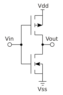
Complementary metal–oxide–semiconductor (CMOS), also known as complementary-symmetry metal–oxide–semiconductor (COS-MOS), is a type of metal–oxide–semiconductor field-effect transistor (MOSFET) fabrication process that uses complementary and symmetrical pairs of p-type and n-type MOSFETs for logic functions. CMOS technology is used for constructing integrated circuit (IC) chips, including microprocessors, microcontrollers, memory chips, and other digital logic circuits, and replaced earlier transistor-transistor logic (TTL) technology.
Electronic design automation (EDA), also referred to as electronic computer-aided design (ECAD), is a category of software tools for designing electronic systems such as integrated circuits and printed circuit boards. The tools work together in a design flow that chip designers use to design and analyze entire semiconductor chips. Since a modern semiconductor chip can have billions of components, EDA tools are essential for their design.
ATPG is an electronic design automation method/technology used to find an input sequence that, when applied to a digital circuit, enables automatic test equipment to distinguish between the correct circuit behavior and the faulty circuit behavior caused by defects. The generated patterns are used to test semiconductor devices after manufacture, or to assist with determining the cause of failure. The effectiveness of ATPG is measured by the number of modeled defects, or fault models, detectable and by the number of generated patterns. These metrics generally indicate test quality and test application time. ATPG efficiency is another important consideration that is influenced by the fault model under consideration, the type of circuit under test, the level of abstraction used to represent the circuit under test, and the required test quality.
A fault model is an engineering model of something that could go wrong in the construction or operation of a piece of equipment. From the model, the designer or user can then predict the consequences of this particular fault. Fault models can be used in almost all branches of engineering.
In computer engineering, a logic family may refer to one of two related concepts. A logic family of monolithic digital integrated circuit devices is a group of electronic logic gates constructed using one of several different designs, usually with compatible logic levels and power supply characteristics within a family. Many logic families were produced as individual components, each containing one or a few related basic logical functions, which could be used as "building-blocks" to create systems or as so-called "glue" to interconnect more complex integrated circuits. A "logic family" may also refer to a set of techniques used to implement logic within VLSI integrated circuits such as central processors, memories, or other complex functions. Some such logic families use static techniques to minimize design complexity. Other such logic families, such as domino logic, use clocked dynamic techniques to minimize size, power consumption and delay.
A mixed-signal integrated circuit is any integrated circuit that has both analog circuits and digital circuits on a single semiconductor die. In real-life applications mixed-signal designs are everywhere, for example, smart mobile phones. Mixed-signal ICs also process both analog and digital signals together. For example, an analog-to-digital converter is a mixed-signal circuit. Mixed-signal circuits or systems are typically cost-effective solutions for building any modern consumer electronics applications.
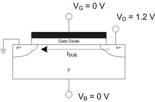
Subthreshold conduction or subthreshold leakage or subthreshold drain current is the current between the source and drain of a MOSFET when the transistor is in subthreshold region, or weak-inversion region, that is, for gate-to-source voltages below the threshold voltage. The terminology for various degrees of inversion is described in Tsividis.
A stuck-at fault is a particular fault model used by fault simulators and automatic test pattern generation (ATPG) tools to mimic a manufacturing defect within an integrated circuit. Individual signals and pins are assumed to be stuck at Logical '1', '0' and 'X'. For example, an input is tied to a logical 1 state during test generation to assure that a manufacturing defect with that type of behavior can be found with a specific test pattern. Likewise the input could be tied to a logical 0 to model the behavior of a defective circuit that cannot switch its output pin. Not all faults can be analyzed using the stuck-at fault model. Compensation for static hazards, namely branching signals, can render a circuit untestable using this model. Also, redundant circuits cannot be tested using this model, since by design there is no change in any output as a result of a single fault.
Design for testing or design for testability (DFT) consists of IC design techniques that add testability features to a hardware product design. The added features make it easier to develop and apply manufacturing tests to the designed hardware. The purpose of manufacturing tests is to validate that the product hardware contains no manufacturing defects that could adversely affect the product's correct functioning.
Power optimization is the use of electronic design automation tools to optimize (reduce) the power consumption of a digital design, such as that of an integrated circuit, while preserving the functionality.
Scan chain is a technique used in design for testing. The objective is to make testing easier by providing a simple way to set and observe every flip-flop in an IC.The basic structure of scan include the following set of signals in order to control and observe the scan mechanism.
- Scan_in and scan_out define the input and output of a scan chain. In a full scan mode usually each input drives only one chain and scan out observe one as well.
- A scan enable pin is a special signal that is added to a design. When this signal is asserted, every flip-flop in the design is connected into a long shift register.
- Clock signal which is used for controlling all the FFs in the chain during shift phase and the capture phase. An arbitrary pattern can be entered into the chain of flip-flops, and the state of every flip-flop can be read out.
In integrated circuit design, dynamic logic is a design methodology in combinatory logic circuits, particularly those implemented in MOS technology. It is distinguished from the so-called static logic by exploiting temporary storage of information in stray and gate capacitances. It was popular in the 1970s and has seen a recent resurgence in the design of high speed digital electronics, particularly computer CPUs. Dynamic logic circuits are usually faster than static counterparts, and require less surface area, but are more difficult to design. Dynamic logic has a higher toggle rate than static logic but the capacitive loads being toggled are smaller so the overall power consumption of dynamic logic may be higher or lower depending on various tradeoffs. When referring to a particular logic family, the dynamic adjective usually suffices to distinguish the design methodology, e.g. dynamic CMOS or dynamic SOI design.
In integrated circuits, electrical power is distributed to the components of the chip over a network of conductors on the chip. Power network design includes the analysis and design of such networks. As in all engineering, this involves tradeoffs - the network must have adequate performance, be sufficiently reliable, but should not use more resources than required.
Multi-threshold CMOS (MTCMOS) is a variation of CMOS chip technology which has transistors with multiple threshold voltages (Vth) in order to optimize delay or power. The Vth of a MOSFET is the gate voltage where an inversion layer forms at the interface between the insulating layer (oxide) and the substrate (body) of the transistor. Low Vth devices switch faster, and are therefore useful on critical delay paths to minimize clock periods. The penalty is that low Vth devices have substantially higher static leakage power. High Vth devices are used on non-critical paths to reduce static leakage power without incurring a delay penalty. Typical high Vth devices reduce static leakage by 10 times compared with low Vth devices.
Low-power electronics are electronics, such as notebook processors, that have been designed to use less electric power than usual, often at some expense. In the case of notebook processors, this expense is processing power; notebook processors tend to consume less power than their desktop counterparts, at the expense of lower processing power.
The MIL-STD-883 standard establishes uniform methods, controls, and procedures for testing microelectronic devices suitable for use within military and aerospace electronic systems including basic environmental tests to determine resistance to deleterious effects of natural elements and conditions surrounding military and space operations; mechanical and electrical tests; workmanship and training procedures; and such other controls and constraints as have been deemed necessary to ensure a uniform level of quality and reliability suitable to the intended applications of those devices. For the purpose of this standard, the term "devices" includes such items as monolithic, multichip, film and hybrid microcircuits, microcircuit arrays, and the elements from which the circuits and arrays are formed. This standard is intended to apply only to microelectronic devices.
Power gating is a technique used in integrated circuit design to reduce power consumption, by shutting off the current to blocks of the circuit that are not in use. In addition to reducing stand-by or leakage power, power gating has the benefit of enabling Iddq testing.
In electronics, pass transistor logic (PTL) describes several logic families used in the design of integrated circuits. It reduces the count of transistors used to make different logic gates, by eliminating redundant transistors. Transistors are used as switches to pass logic levels between nodes of a circuit, instead of as switches connected directly to supply voltages. This reduces the number of active devices, but has the disadvantage that the difference of the voltage between high and low logic levels decreases at each stage. Each transistor in series is less saturated at its output than at its input. If several devices are chained in series in a logic path, a conventionally constructed gate may be required to restore the signal voltage to the full value. By contrast, conventional CMOS logic switches transistors so the output connects to one of the power supply rails, so logic voltage levels in a sequential chain do not decrease. Simulation of circuits may be required to ensure adequate performance.
References
Straka, B.; Manhaeve, Hans; Vanneuville, J.; Svajda, M. (1998). "A fully digital controlled off-chip IDDQ measurement unit.". Proceedings -Design, Automation and Test in Europe, DATE. Design, Automation and Test in Europe. pp. 495–500.
Sabade, Sagar; Walker, D.M.H. (June 2004). "IDDX -based test methods: A survey". ACM Transactions on Design Automation of Electronic Systems. 9 (2): 159–198. Retrieved 11 November 2018.