Related Research Articles
The Defense Advanced Research Projects Agency (DARPA) is a research and development agency of the United States Department of Defense responsible for the development of emerging technologies for use by the military.

MEMS is the technology of microscopic devices incorporating both electronic and moving parts. MEMS are made up of components between 1 and 100 micrometres in size, and MEMS devices generally range in size from 20 micrometres to a millimetre, although components arranged in arrays can be more than 1000 mm2. They usually consist of a central unit that processes data and several components that interact with the surroundings.

An embedded system is a computer system—a combination of a computer processor, computer memory, and input/output peripheral devices—that has a dedicated function within a larger mechanical or electronic system. It is embedded as part of a complete device often including electrical or electronic hardware and mechanical parts. Because an embedded system typically controls physical operations of the machine that it is embedded within, it often has real-time computing constraints. Embedded systems control many devices in common use. In 2009, it was estimated that ninety-eight percent of all microprocessors manufactured were used in embedded systems.

Software-defined radio (SDR) is a radio communication system where components that conventionally have been implemented in analog hardware are instead implemented by means of software on a personal computer or embedded system. While the concept of SDR is not new, the rapidly evolving capabilities of digital electronics render practical many processes which were once only theoretically possible.

Photonics is a branch of optics that involves the application of generation, detection, and manipulation of light in form of photons through emission, transmission, modulation, signal processing, switching, amplification, and sensing. Photonics is closely related to quantum electronics, where quantum electronics deals with the theoretical part of it while photonics deal with its engineering applications. Though covering all light's technical applications over the whole spectrum, most photonic applications are in the range of visible and near-infrared light. The term photonics developed as an outgrowth of the first practical semiconductor light emitters invented in the early 1960s and optical fibers developed in the 1970s.
Electronic design automation (EDA), also referred to as electronic computer-aided design (ECAD), is a category of software tools for designing electronic systems such as integrated circuits and printed circuit boards. The tools work together in a design flow that chip designers use to design and analyze entire semiconductor chips. Since a modern semiconductor chip can have billions of components, EDA tools are essential for their design; this article in particular describes EDA specifically with respect to integrated circuits (ICs).

A ball grid array (BGA) is a type of surface-mount packaging used for integrated circuits. BGA packages are used to permanently mount devices such as microprocessors. A BGA can provide more interconnection pins than can be put on a dual in-line or flat package. The whole bottom surface of the device can be used, instead of just the perimeter. The traces connecting the package's leads to the wires or balls which connect the die to package are also on average shorter than with a perimeter-only type, leading to better performance at high speeds.

Analog Devices, Inc. (ADI), also known simply as Analog, is an American multinational semiconductor company specializing in data conversion, signal processing, and power management technology, headquartered in Wilmington, Massachusetts.

A handheld projector is an image projector in a handheld device. It was developed as a computer display device for compact portable devices such as mobile phones, personal digital assistants, and digital cameras, which have sufficient storage capacity to handle presentation materials but are too small to accommodate a display screen that an audience can see easily. Handheld projectors involve miniaturized hardware, and software that can project digital images onto a nearby viewing surface.
Brain implants, often referred to as neural implants, are technological devices that connect directly to a biological subject's brain – usually placed on the surface of the brain, or attached to the brain's cortex. A common purpose of modern brain implants and the focus of much current research is establishing a biomedical prosthesis circumventing areas in the brain that have become dysfunctional after a stroke or other head injuries. This includes sensory substitution, e.g., in vision. Other brain implants are used in animal experiments simply to record brain activity for scientific reasons. Some brain implants involve creating interfaces between neural systems and computer chips. This work is part of a wider research field called brain–computer interfaces.
Masklesslithography (MPL) is a photomask-less photolithography-like technology used to project or focal-spot write the image pattern onto a chemical resist-coated substrate by means of UV radiation or electron beam.
A soft microprocessor is a microprocessor core that can be wholly implemented using logic synthesis. It can be implemented via different semiconductor devices containing programmable logic, including both high-end and commodity variations.
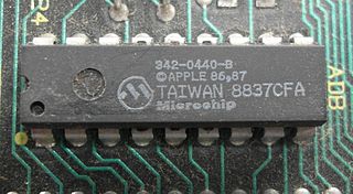
Microchip Technology Inc. is a publicly listed American corporation that manufactures microcontroller, mixed-signal, analog, and Flash-IP integrated circuits. Its products include microcontrollers, Serial EEPROM devices, Serial SRAM devices, embedded security devices, radio frequency (RF) devices, thermal, power and battery management analog devices, as well as linear, interface and wireless products.
The School of Engineering and Applied Science (SEAS) at the George Washington University in Washington, D.C. is a technical school which specializes in engineering, technology, communications, and transportation. The school is located on the main campus of the George Washington University and offers both undergraduate and graduate programs.
A photonic integrated circuit (PIC) or integrated optical circuit is a microchip containing two or more photonic components which form a functioning circuit. This technology detects, generates, transports, and processes light. Photonic integrated circuits utilize photons as opposed to electrons that are utilized by electronic integrated circuits. The major difference between the two is that a photonic integrated circuit provides functions for information signals imposed on optical wavelengths typically in the visible spectrum or near infrared (850–1650 nm).

Multi-project chip (MPC), and multi-project wafer (MPW) semiconductor manufacturing arrangements allow customers to share mask and microelectronics wafer fabrication cost between several designs or projects.
A massively parallel processor array, also known as a multi purpose processor array (MPPA) is a type of integrated circuit which has a massively parallel array of hundreds or thousands of CPUs and RAM memories. These processors pass work to one another through a reconfigurable interconnect of channels. By harnessing a large number of processors working in parallel, an MPPA chip can accomplish more demanding tasks than conventional chips. MPPAs are based on a software parallel programming model for developing high-performance embedded system applications.
The IEEE International Electron Devices Meeting (IEDM) is an annual micro- and nanoelectronics conference held each December that serves as a forum for reporting technological breakthroughs in the areas of semiconductor and related device technologies, design, manufacturing, physics, modeling and circuit-device interaction.
The Photonically Optimized Embedded Microprocessors (POEM) is DARPA program. It should demonstrate photonic technologies that can be integrated within embedded microprocessors and enable energy-efficient high-capacity communications between the microprocessor and DRAM. For realizing POEM technology CMOS and DRAM-compatible photonic links should operate at high bit-rates with very low power dissipation.

The metal–oxide–semiconductor field-effect transistor, also known as the metal–oxide–silicon transistor, is a type of insulated-gate field-effect transistor (IGFET) that is fabricated by the controlled oxidation of a semiconductor, typically silicon. The voltage of the covered gate determines the electrical conductivity of the device; this ability to change conductivity with the amount of applied voltage can be used for amplifying or switching electronic signals.
References
- ↑ "MEMS". DARPA MTO. Archived from the original on 2011-03-05. Retrieved 2012-08-26.
- ↑ "Electronics". DARPA MTO. Archived from the original on 2012-12-12. Retrieved 2012-08-26.
- ↑ "Algorithms". DARPA MTO. Archived from the original on 2012-06-03. Retrieved 2012-08-26.
- ↑ "Architectures". DARPA MTO. Archived from the original on 2012-06-03. Retrieved 2012-08-26.
- ↑ "Photonics". DARPA MTO. Archived from the original on 2012-09-15. Retrieved 2012-08-26.
- ↑ Shachtman, Noah (2012-07-10). "Exclusive: Darpa Gets a New Boss, and Solyndra Is in Her Past". Wired . Retrieved 2012-08-25.
- ↑ https://www.darpa.mil/staff/dr-mark-rosker.
{{cite web}}: Missing or empty|title=(help)