Nanotechnology is the manipulation of matter with at least one dimension sized from 1 to 100 nanometers (nm). At this scale, commonly known as the nanoscale, surface area and quantum mechanical effects become important in describing properties of matter. This definition of nanotechnology includes all types of research and technologies that deal with these special properties. It is common to see the plural form "nanotechnologies" as well as "nanoscale technologies" to refer to research and applications whose common trait is scale. An earlier understanding of nanotechnology referred to the particular technological goal of precisely manipulating atoms and molecules for fabricating macroscale products, now referred to as molecular nanotechnology.
Nanoengineering is the practice of engineering on the nanoscale. It derives its name from the nanometre, a unit of measurement equalling one billionth of a meter.
Nanoid robotics, or for short, nanorobotics or nanobotics, is an emerging technology field creating machines or robots, which are called nanorobots or simply nanobots, whose components are at or near the scale of a nanometer. More specifically, nanorobotics refers to the nanotechnology engineering discipline of designing and building nanorobots with devices ranging in size from 0.1 to 10 micrometres and constructed of nanoscale or molecular components. The terms nanobot, nanoid, nanite, nanomachine and nanomite have also been used to describe such devices currently under research and development.
The National Nanotechnology Initiative (NNI) is a research and development initiative which provides a framework to coordinate nanoscale research and resources among United States federal government agencies and departments.

Dip pen nanolithography (DPN) is a scanning probe lithography technique where an atomic force microscope (AFM) tip is used to directly create patterns on a substrate. It can be done on a range of substances with a variety of inks. A common example of this technique is exemplified by the use of alkane thiolates to imprint onto a gold surface. This technique allows surface patterning on scales of under 100 nanometers. DPN is the nanotechnology analog of the dip pen, where the tip of an atomic force microscope cantilever acts as a "pen", which is coated with a chemical compound or mixture acting as an "ink", and put in contact with a substrate, the "paper".
Nanomanufacturing is both the production of nanoscaled materials, which can be powders or fluids, and the manufacturing of parts "bottom up" from nanoscaled materials or "top down" in smallest steps for high precision, used in several technologies such as laser ablation, etching and others. Nanomanufacturing differs from molecular manufacturing, which is the manufacture of complex, nanoscale structures by means of nonbiological mechanosynthesis.
The history of nanotechnology traces the development of the concepts and experimental work falling under the broad category of nanotechnology. Although nanotechnology is a relatively recent development in scientific research, the development of its central concepts happened over a longer period of time. The emergence of nanotechnology in the 1980s was caused by the convergence of experimental advances such as the invention of the scanning tunneling microscope in 1981 and the discovery of fullerenes in 1985, with the elucidation and popularization of a conceptual framework for the goals of nanotechnology beginning with the 1986 publication of the book Engines of Creation. The field was subject to growing public awareness and controversy in the early 2000s, with prominent debates about both its potential implications as well as the feasibility of the applications envisioned by advocates of molecular nanotechnology, and with governments moving to promote and fund research into nanotechnology. The early 2000s also saw the beginnings of commercial applications of nanotechnology, although these were limited to bulk applications of nanomaterials rather than the transformative applications envisioned by the field.
The impact of nanotechnology extends from its medical, ethical, mental, legal and environmental applications, to fields such as engineering, biology, chemistry, computing, materials science, and communications.
The following outline is provided as an overview of and topical guide to nanotechnology:

Chad Alexander Mirkin is an American chemist. He is the George B. Rathmann professor of chemistry, professor of medicine, professor of materials science and engineering, professor of biomedical engineering, and professor of chemical and biological engineering, and director of the International Institute for Nanotechnology and Center for Nanofabrication and Molecular Self-Assembly at Northwestern University.
Green nanotechnology refers to the use of nanotechnology to enhance the environmental sustainability of processes producing negative externalities. It also refers to the use of the products of nanotechnology to enhance sustainability. It includes making green nano-products and using nano-products in support of sustainability.
The societal impact of nanotechnology are the potential benefits and challenges that the introduction of novel nanotechnological devices and materials may hold for society and human interaction. The term is sometimes expanded to also include nanotechnology's health and environmental impact, but this article will only consider the social and political impact of nanotechnology.
The College of Nanotechnology, Science, and Engineering is part of the University at Albany, SUNY in Albany, New York. Founded in 2004 at the University at Albany, SUNY, the college underwent rapid expansion in the late-2000s and early-2010s before merging with the SUNY Institute of Technology in 2014. The college rejoined the University at Albany in 2023. The college was the first college in the United States devoted to nanotechnology.
NanoScale Corporation was a private US corporation, located in Manhattan, Kansas. It was founded by Dr. Kenneth J. Klabunde in 1995, as Nantek, Inc., to further develop and commercialize certain intellectual properties of Kansas State University. In January 2001, the Company’s name was changed to NanoScale Materials, Inc. They were reincorporated in July 2007, as a Delaware corporation, with the current name NanoScale Corporation. NanoScale worked with a variety of private, commercial, and government customers. NanoScale developed, manufactured, and sold nano-crystalline metal oxides and other materials for a wide array of applications, including odor neutralization, hazardous chemical neutralization, and environmental remediation. Scientists affiliated with NanoScale Corporation have collaborated to write, and publish, many scientific papers and publications in the subjects of material science and advanced chemistry nanotechnology. They closed down following wire-fraud.
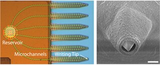
A nanofountain probe (NFP) is a device for 'drawing' micropatterns of liquid chemicals at extremely small resolution. An NFP contains a cantilevered micro-fluidic device terminated in a nanofountain. The embedded microfluidics facilitates rapid and continuous delivery of molecules from the on-chip reservoirs to the fountain tip. When the tip is brought into contact with the substrate, a liquid meniscus forms, providing a path for molecular transport to the substrate. By controlling the geometry of the meniscus through hold time and deposition speed, various inks and biomolecules could be patterned on a surface, with sub 100 nm resolution.

Mark Christopher Hersam is a professor of Chemistry and Materials Science Engineering at Northwestern University (2000–present) who, according to the National Science Foundation, has made "major breakthrough[s]" in the field of nanotechnology. He is a 2014 recipient of the MacArthur "Genius" Award and a 1996 Marshall Scholar. He is also an Executive Editor of ACS Nano. As of October 2023, he has been cited over 68,000 times according to Google Scholar.
The ISO/TS 80004 series of standards, from the International Organization for Standardization, describe vocabulary for nanotechnology and its applications. These were largely motivated by health, safety and environment concerns, many of them originally elaborated by Eric Drexler in his 1985 Engines of Creation and echoed in more recent research. The ISO standards simply describe vocabulary or terminology by which a number of critical discussions between members of various stakeholder communities, including the public and political leaders, can begin. Drexler, in Chapter 15 of his 1985 work, explained how such consultation and the evolution of new social media and mechanisms to make objective scientific determinations regardless of political and industrial and public pressures, would be important to the evolution of the field. Nonetheless, it took a quarter-century for the ISO to agree and eventually standardize on this terminology.
The International Institute for Nanotechnology (IIN) was established by Northwestern University in 2000. It was the first institute of its kind in the United States and is one of the premier nanoscience research centers in the world. Today, the IIN represents and unites more than $1 billion in nanotechnology research, educational programs, and supporting infrastructure.
This glossary of nanotechnology is a list of definitions of terms and concepts relevant to nanotechnology, its sub-disciplines, and related fields.