Related Research Articles

A photoresist is a light-sensitive material used in several processes, such as photolithography and photoengraving, to form a patterned coating on a surface. This process is crucial in the electronics industry.
In organometallic chemistry, organolithium reagents are chemical compounds that contain carbon–lithium (C–Li) bonds. These reagents are important in organic synthesis, and are frequently used to transfer the organic group or the lithium atom to the substrates in synthetic steps, through nucleophilic addition or simple deprotonation. Organolithium reagents are used in industry as an initiator for anionic polymerization, which leads to the production of various elastomers. They have also been applied in asymmetric synthesis in the pharmaceutical industry. Due to the large difference in electronegativity between the carbon atom and the lithium atom, the C−Li bond is highly ionic. Owing to the polar nature of the C−Li bond, organolithium reagents are good nucleophiles and strong bases. For laboratory organic synthesis, many organolithium reagents are commercially available in solution form. These reagents are highly reactive, and are sometimes pyrophoric.

Self-assembled monolayers (SAM) of organic molecules are molecular assemblies formed spontaneously on surfaces by adsorption and are organized into more or less large ordered domains. In some cases molecules that form the monolayer do not interact strongly with the substrate. This is the case for instance of the two-dimensional supramolecular networks of e.g. perylenetetracarboxylic dianhydride (PTCDA) on gold or of e.g. porphyrins on highly oriented pyrolitic graphite (HOPG). In other cases the molecules possess a head group that has a strong affinity to the substrate and anchors the molecule to it. Such a SAM consisting of a head group, tail and functional end group is depicted in Figure 1. Common head groups include thiols, silanes, phosphonates, etc.

Dip pen nanolithography (DPN) is a scanning probe lithography technique where an atomic force microscope (AFM) tip is used to create patterns directly on a range of substances with a variety of inks. A common example of this technique is exemplified by the use of alkane thiolates to imprint onto a gold surface. This technique allows surface patterning on scales of under 100 nanometers. DPN is the nanotechnology analog of the dip pen, where the tip of an atomic force microscope cantilever acts as a "pen," which is coated with a chemical compound or mixture acting as an "ink," and put in contact with a substrate, the "paper."
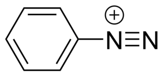
Diazonium compounds or diazonium salts are a group of organic compounds sharing a common functional group [R−N+≡N]X− where R can be any organic group, such as an alkyl or an aryl, and X is an inorganic or organic anion, such as a halide.
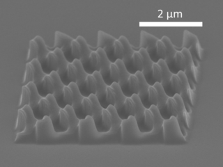
Nanoimprint lithography (NIL) is a method of fabricating nanometer scale patterns. It is a simple nanolithography process with low cost, high throughput and high resolution. It creates patterns by mechanical deformation of imprint resist and subsequent processes. The imprint resist is typically a monomer or polymer formulation that is cured by heat or UV light during the imprinting. Adhesion between the resist and the template is controlled to allow proper release.

Surface-enhanced Raman spectroscopy or surface-enhanced Raman scattering (SERS) is a surface-sensitive technique that enhances Raman scattering by molecules adsorbed on rough metal surfaces or by nanostructures such as plasmonic-magnetic silica nanotubes. The enhancement factor can be as much as 1010 to 1011, which means the technique may detect single molecules.
A solvated electron is a free electron in a solution, and is the smallest possible anion. Solvated electrons occur widely. Often, discussions of solvated electrons focus on their solutions in ammonia, which are stable for days, but solvated electrons also occur in water and other solvents – in fact, in any solvent that mediates outer-sphere electron transfer. The solvated electron is responsible for a great deal of radiation chemistry.

Tetramethylammonium hydroxide (TMAH or TMAOH) is a quaternary ammonium salt with molecular formula N(CH3)4+ OH−. It is commonly encountered in form of concentrated solutions in water or methanol. TMAH in solid state and its aqueous solutions are all colorless, but may be yellowish if impure. Although TMAH has virtually no odor when pure, samples often have a strong fishy smell due to presence of trimethylamine which is a common impurity. TMAH has several diverse industrial and research applications.

Microcontact printing is a form of soft lithography that uses the relief patterns on a master polydimethylsiloxane (PDMS) stamp or Urethane rubber micro stamp to form patterns of self-assembled monolayers (SAMs) of ink on the surface of a substrate through conformal contact as in the case of nanotransfer printing (nTP). Its applications are wide-ranging including microelectronics, surface chemistry and cell biology.

Printed electronics is a set of printing methods used to create electrical devices on various substrates. Printing typically uses common printing equipment suitable for defining patterns on material, such as screen printing, flexography, gravure, offset lithography, and inkjet. By electronic-industry standards, these are low-cost processes. Electrically functional electronic or optical inks are deposited on the substrate, creating active or passive devices, such as thin film transistors; capacitors; coils; resistors. Some researchers expect printed electronics to facilitate widespread, very low-cost, low-performance electronics for applications such as flexible displays, smart labels, decorative and animated posters, and active clothing that do not require high performance.
Chain transfer is a polymerization reaction by which the activity of a growing polymer chain is transferred to another molecule.
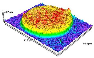
Sarfus is an optical quantitative imaging technique based on the association of:
Scanning electrochemical microscopy (SECM) is a technique within the broader class of scanning probe microscopy (SPM) that is used to measure the local electrochemical behavior of liquid/solid, liquid/gas and liquid/liquid interfaces. Initial characterization of the technique was credited to University of Texas electrochemist, Allen J. Bard, in 1989. Since then, the theoretical underpinnings have matured to allow widespread use of the technique in chemistry, biology and materials science. Spatially resolved electrochemical signals can be acquired by measuring the current at an ultramicroelectrode (UME) tip as a function of precise tip position over a substrate region of interest. Interpretation of the SECM signal is based on the concept of diffusion-limited current. Two-dimensional raster scan information can be compiled to generate images of surface reactivity and chemical kinetics.
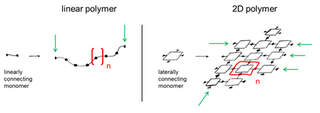
A two-dimensional polymer (2DP) is a sheet-like monomolecular macromolecule consisting of laterally connected repeat units with end groups along all edges. This recent definition of 2DP is based on Hermann Staudinger's polymer concept from the 1920s. According to this, covalent long chain molecules ("Makromoleküle") do exist and are composed of a sequence of linearly connected repeat units and end groups at both termini.
The surface chemistry of paper is responsible for many important paper properties, such as gloss, waterproofing, and printability. Many components are used in the paper-making process that affect the surface.

David Lyndon Emsley FRSC is a British chemist specialising in solid-state nuclear magnetic resonance and a professor at EPFL. He was awarded the 2012 Grand Prix Charles-Leopold Mayer of the French Académie des Sciences and the 2015 Bourke Award of the Royal Society of Chemistry.

Yueh-Lin (Lynn) Loo is a Malaysian-born chemical engineer and the Theodora D. '78 and William H. Walton III '74 Professor in Engineering at Princeton University, where she is also the Director of the Andlinger Center for Energy and the Environment. She is known for inventing nanotransfer printing. Loo was elected a Fellow of the Materials Research Society in 2020.
In homogeneous catalysis, C2-symmetric ligands refer to ligands that lack mirror symmetry but have C2 symmetry. Such ligands are usually bidentate and are valuable in catalysis. The C2 symmetry of ligands limits the number of possible reaction pathways and thereby increases enantioselectivity, relative to asymmetrical analogues. C2-symmetric ligands are a subset of chiral ligands. Chiral ligands, including C2-symmetric ligands, combine with metals or other groups to form chiral catalysts. These catalysts engage in enantioselective chemical synthesis, in which chirality in the catalyst yields chirality in the reaction product.
Jingdong Zhang was a Chinese–Danish chemist and Professor of Chemistry at the Technical University of Denmark. Her research considered nanochemistry and the novel materials for catalysis, as well as the development of advanced characterisation techniques such as scanning tunnelling microscopy and atomic force microscopy. She was elected to the Akademiet for de Tekniske Videnskaber in 2017.
References
- 1 2 Loo, Y; Willett, R.; Baldwin, K.; Rogers, J. (2002). "Interfacial Chemistries for Nanoscale Transfer Printing". J. Am. Chem. Soc. 124 (26): 7654–7655. doi:10.1021/ja026355v.
- ↑ Bhusan, Bharat (2010). Springer Handbook of Nanotechnology. New York: Springer. pp. 313–332.
- ↑ Bhandari, D.; Kravchenko, I.; Lavrik, N.; Sepaniak, M (2011). "Nanotransfer Printing Using Plasma Eched Silicon Stamps and Mediated by in situ Deposited Fluoropolymer". J. Am. Chem. Soc. 133 (20): 7722–7724. doi:10.1021/ja201497a. PMID 21526774.
- ↑ "Yueh-Lin (Lynn) Loo, 30". MIT Technology Review . 2004. Retrieved November 15, 2015.