Related Research Articles

A crystallographic defect is an interruption of the regular patterns of arrangement of atoms or molecules in crystalline solids. The positions and orientations of particles, which are repeating at fixed distances determined by the unit cell parameters in crystals, exhibit a periodic crystal structure, but this is usually imperfect. Several types of defects are often characterized: point defects, line defects, planar defects, bulk defects. Topological homotopy establishes a mathematical method of characterization.
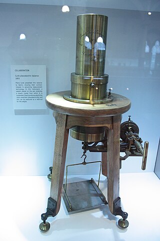
Piezoelectricity is the electric charge that accumulates in certain solid materials—such as crystals, certain ceramics, and biological matter such as bone, DNA, and various proteins—in response to applied mechanical stress. The word piezoelectricity means electricity resulting from pressure and latent heat. It is derived from Ancient Greek πιέζω (piézō) 'to squeeze or press', and ἤλεκτρον (ḗlektron) 'amber'. The German form of the word (Piezoelektricität) was coined in 1881 by the German physicist Wilhelm Gottlieb Hankel; the English word was coined in 1883.
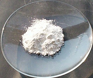
Zinc oxide is an inorganic compound with the formula ZnO. It is a white powder which is insoluble in water. ZnO is used as an additive in numerous materials and products including cosmetics, food supplements, rubbers, plastics, ceramics, glass, cement, lubricants, paints, sunscreens, ointments, adhesives, sealants, pigments, foods, batteries, ferrites, fire retardants, semi conductors, and first-aid tapes. Although it occurs naturally as the mineral zincite, most zinc oxide is produced synthetically.

Cadmium sulfide is the inorganic compound with the formula CdS. Cadmium sulfide is a yellow salt. It occurs in nature with two different crystal structures as the rare minerals greenockite and hawleyite, but is more prevalent as an impurity substituent in the similarly structured zinc ores sphalerite and wurtzite, which are the major economic sources of cadmium. As a compound that is easy to isolate and purify, it is the principal source of cadmium for all commercial applications. Its vivid yellow color led to its adoption as a pigment for the yellow paint "cadmium yellow" in the 18th century.
Aluminium nitride (AlN) is a solid nitride of aluminium. It has a high thermal conductivity of up to 321 W/(m·K) and is an electrical insulator. Its wurtzite phase (w-AlN) has a band gap of ~6 eV at room temperature and has a potential application in optoelectronics operating at deep ultraviolet frequencies.
A superlattice is a periodic structure of layers of two materials. Typically, the thickness of one layer is several nanometers. It can also refer to a lower-dimensional structure such as an array of quantum dots or quantum wells.
Multiferroics are defined as materials that exhibit more than one of the primary ferroic properties in the same phase:
SIESTA is an original method and its computer program implementation, to efficiently perform electronic structure calculations and ab initio molecular dynamics simulations of molecules and solids. SIESTA uses strictly localized basis sets and the implementation of linear-scaling algorithms. Accuracy and speed can be set in a wide range, from quick exploratory calculations to highly accurate simulations matching the quality of other approaches, such as the plane-wave and all-electron methods.

Boron arsenide is a chemical compound involving boron and arsenic, usually with a chemical formula BAs. Other boron arsenide compounds are known, such as the subarsenide B12As2. Chemical synthesis of cubic BAs is very challenging and its single crystal forms usually have defects.
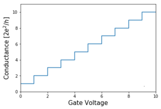
A quantum point contact (QPC) is a narrow constriction between two wide electrically conducting regions, of a width comparable to the electronic wavelength.
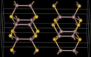
Gallium(II) sulfide, GaS, is a chemical compound of gallium and sulfur. The normal form of gallium(II) sulfide as made from the elements has a hexagonal layer structure containing Ga24+ units which have a Ga-Ga distance of 248pm. This layer structure is similar to GaTe, GaSe and InSe. An unusual metastable form, with a distorted wurtzite structure has been reported as being produced using MOCVD. The metal organic precursors were di-tert-butyl gallium dithiocarbamates, for example GatBu2(S2CNMe2) and this was deposited onto GaAs. The structure of the GaS produced in this way is presumably Ga2+ S2−.

Diindenoperylene (DIP) is an organic semiconductor which receives attention because of its potential application in optoelectronics (solar cells, OLEDs) and electronics (RFID tags). DIP is a planar perylene derivative with two indeno-groups attached to opposite sides of the perylene core. Its chemical formula is C32H16, the full chemical name is diindeno[1,2,3-cd:1',2',3'-lm]perylene. Its chemical synthesis has been described.
Gallium manganese arsenide, chemical formula (Ga,Mn)As is a magnetic semiconductor. It is based on the world's second most commonly used semiconductor, gallium arsenide,, and readily compatible with existing semiconductor technologies. Differently from other dilute magnetic semiconductors, such as the majority of those based on II-VI semiconductors, it is not paramagnetic but ferromagnetic, and hence exhibits hysteretic magnetization behavior. This memory effect is of importance for the creation of persistent devices. In (Ga,Mn)As, the manganese atoms provide a magnetic moment, and each also acts as an acceptor, making it a p-type material. The presence of carriers allows the material to be used for spin-polarized currents. In contrast, many other ferromagnetic magnetic semiconductors are strongly insulating and so do not possess free carriers. (Ga,Mn)As is therefore a candidate material for spintronic devices but it is likely to remain only a testbed for basic research as its Curie temperature could only be raised up to approximatelly 200 K.

Positron annihilation spectroscopy (PAS) or sometimes specifically referred to as positron annihilation lifetime spectroscopy (PALS) is a non-destructive spectroscopy technique to study voids and defects in solids.
Gallium(II) selenide (GaSe) is a chemical compound. It has a hexagonal layer structure, similar to that of GaS. It is a photoconductor, a second harmonic generation crystal in nonlinear optics, and has been used as a far-infrared conversion material at 14–31 THz and above.

In condensed-matter physics, a collision cascade is a set of nearby adjacent energetic collisions of atoms induced by an energetic particle in a solid or liquid.
In its most general form, the magnetoelectric effect (ME) denotes any coupling between the magnetic and the electric properties of a material. The first example of such an effect was described by Wilhelm Röntgen in 1888, who found that a dielectric material moving through an electric field would become magnetized. A material where such a coupling is intrinsically present is called a magnetoelectric.
Piezotronics effect is using the piezoelectric potential (piezopotential) created in materials with piezoelectricity as a “gate” voltage to tune/control the charge carrier transport properties for fabricating new devices.

Vladimir G. Dubrovskii is the head of Laboratory of physics of nanostructures at St. Petersburg Academic University, a leading research scientist at Ioffe Institute, and a professor at St. Petersburg State University and ITMO University.

Anna Fontcuberta i Morral is a Spanish and Swiss physicist and materials scientist. Her research focuses on nanotechnology applied in the production of solar cells. She is a full professor at École Polytechnique Fédérale de Lausanne (EPFL) and the head of the Laboratory of Semiconductor Materials.
References
- ↑ André, Régis; J. Cibert; Le Si Dang; J. Zeman; M. Zigone (1996). "Nonlinear piezoelectricity: The effect of pressure on CdTe". Physical Review B. 53 (11): 6951–6954. doi:10.1103/PhysRevB.53.6951.
- ↑ Migliorato, Max; et al. (2014). "A Review of Non Linear Piezoelectricity in Semiconductors". AIP Conference Proceedings. 1590 (1): 32–41. Bibcode:2014AIPC.1590...32M. doi: 10.1063/1.4870192 .
- ↑ Bester, Gabriel; X. Wu; D. Vanderbilt; A. Zunger (2006). "Importance of Second-Order Piezoelectric Effects in Zinc-Blende Semiconductors". Physical Review Letters. 96 (18): 187602. arXiv: cond-mat/0604596 . Bibcode:2006PhRvL..96r7602B. doi:10.1103/PhysRevLett.96.187602. PMID 16712396. S2CID 10596640.
- ↑ Migliorato, Max; D. Powell; A.G. Cullis; T. Hammerschmidt; G.P. Srivastava (2006). "Composition and strain dependence of the piezoelectric coefficients in InxGa1−xAs alloys". Physical Review B. 74 (24): 245332. Bibcode:2006PhRvB..74x5332M. doi:10.1103/PhysRevB.74.245332. hdl: 11858/00-001M-0000-0011-02EF-0 .
- ↑ Harrison, Walter (1989). Electronic Structure and Properties of Solids. New York: Dover Publications Inc.
- ↑ Garg, Raman; A. Hüe; V. Haxha; M. A. Migliorato; T. Hammerschmidt; G.P. Srivastava (2009). "Tunability of the piezoelectric fields in strained III-V semiconductors". Appl. Phys. Lett. 95 (4): 041912. Bibcode:2009ApPhL..95d1912G. doi: 10.1063/1.3194779 .
- ↑ Tse, Geoffrey; J. Pal; U. Monteverde; R. Garg; V. Haxha; M. A. Migliorato; S. Tomic´ (2013). "Non-Linear Piezoelectricity in Zinc Blende GaAs and InAs Semiconductors". J. Appl. Phys. 114 (7): 073515–073515–12. Bibcode:2013JAP...114g3515T. doi:10.1063/1.4818798. S2CID 14023644.
- ↑ A. Beya-Wakata; et al. (2011). "First- and second-order piezoelectricity in III-V semiconductors". Phys. Rev. B. 84 (19): 195207. Bibcode:2011PhRvB..84s5207B. doi:10.1103/PhysRevB.84.195207.
- ↑ Pal, Joydeep; G. Tse; V. Haxha; M.A. Migliorato; S. Tomic´ (2011). "Non-Linear Piezoelectricity in Zinc Blende GaAs and InAs Semiconductors". Phys. Rev. B. 84 (8): 085211. Bibcode:2011PhRvB..84h5211P. doi:10.1103/PhysRevB.84.085211.
- ↑ L. Pedesseau; C. Katan; J. Even (2012). "On the entanglement of electrostriction and non-linear piezoelectricity in non-centrosymmetric materials" (PDF). Appl. Phys. Lett. 100 (3): 031903. Bibcode:2012ApPhL.100c1903P. doi:10.1063/1.3676666.
- ↑ Al-Zahrani, Hanan; J.Pal; M.A. Migliorato (2013). "Non Linear Piezoelectricity in Wurtzite ZnO Semiconductors". Nano Energy. 2 (6): 1214–1217. doi:10.1016/j.nanoen.2013.05.005.
- ↑ Pierre-Yves Prodhomme; Annie Beya-Wakata; Gabriel Bester (2013). "Nonlinear piezoelectricity in wurtzite semiconductors". Phys. Rev. B. 88 (12): 121304(R). Bibcode:2013PhRvB..88l1304P. doi:10.1103/PhysRevB.88.121304.
- ↑ Al-Zahrani, Hanan; J.Pal; M.A. Migliorato; G. Tse; Dapeng Yu (2015). "Piezoelectric Field Enhancement in III-V Core-Shell Nanowires". Nano Energy. 14: 382–391. doi: 10.1016/j.nanoen.2014.11.046 .
- ↑ Crutchley, Benjamin; I. P. Marko; S. J. Sweeney; J. Pal; M.A. Migliorato (2013). "Optical properties of InGaN-based LEDs investigated using high hydrostatic pressure dependent techniques". Physica Status Solidi B. 250 (4): 698–702. Bibcode:2013PSSBR.250..698C. doi:10.1002/pssb.201200514.
- ↑ Pal, Joydeep; M. A. Migliorato; C.-K. Li; Y.-R. Wu; B. G. Crutchley; I. P. Marko; S. J. Sweeney (2000). "Enhancement of Efficiency of InGaN-based LEDs through Strain and Piezoelectric Field Management". J. Appl. Phys. 114 (3): 073104. Bibcode:2000JChPh.113..987C. doi:10.1063/1.481879.