Related Research Articles

Solder is a fusible metal alloy used to create a permanent bond between metal workpieces. Solder is melted in order to wet the parts of the joint, where it adheres to and connects the pieces after cooling. Metals or alloys suitable for use as solder should have a lower melting point than the pieces to be joined. The solder should also be resistant to oxidative and corrosive effects that would degrade the joint over time. Solder used in making electrical connections also needs to have favorable electrical characteristics.

Electroplating, also known as electrochemical deposition or electrodeposition, is a process for producing a metal coating on a solid substrate through the reduction of cations of that metal by means of a direct electric current. The part to be coated acts as the cathode of an electrolytic cell; the electrolyte is a solution of a salt whose cation is the metal to be coated, and the anode is usually either a block of that metal, or of some inert conductive material. The current is provided by an external power supply.

A printed circuit board (PCB), also called printed wiring board (PWB), is a laminated sandwich structure of conductive and insulating layers, each with a pattern of traces, planes and other features etched from one or more sheet layers of copper laminated onto or between sheet layers of a non-conductive substrate. PCBs are used to connect or "wire" components to one another in an electronic circuit. Electrical components may be fixed to conductive pads on the outer layers, generally by soldering, which both electrically connects and mechanically fastens the components to the board. Another manufacturing process adds vias, metal-lined drilled holes that enable electrical interconnections between conductive layers, to boards with more than a single side.
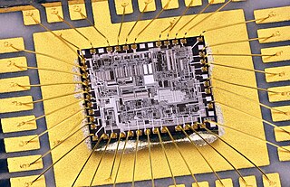
Wire bonding is a method of making interconnections between an integrated circuit (IC) or other semiconductor device and its packaging during semiconductor device fabrication. Wire bonding can also be used to connect an IC to other electronics or to connect from one printed circuit board (PCB) to another, although these are less common. Wire bonding is generally considered the most cost-effective and flexible interconnect technology and is used to assemble the vast majority of semiconductor packages. Wire bonding can be used at frequencies above 100 GHz.
In metallurgy, a flux is a chemical reducing agent, flowing agent, or purifying agent. Fluxes may have more than one function at a time. They are used in both extractive metallurgy and metal joining.

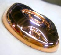
Chrome plating is a technique of electroplating a thin layer of chromium onto a metal object. A chrome plated part is called chrome, or is said to have been chromed. The chromium layer can be decorative, provide corrosion resistance, facilitate cleaning, and increase surface hardness. Sometimes a less expensive substitute for chrome, such as nickel, may be used for aesthetic purposes.
Plating is a finishing process in which a metal is deposited on a surface. Plating has been done for hundreds of years; it is also critical for modern technology. Plating is used to decorate objects, for corrosion inhibition, to improve solderability, to harden, to improve wearability, to reduce friction, to improve paint adhesion, to alter conductivity, to improve IR reflectivity, for radiation shielding, and for other purposes. Jewelry typically uses plating to give a silver or gold finish.
Copper electroplating is the process of electroplating a layer of copper onto the surface of a metal object. Copper is used both as a standalone coating and as an undercoat onto which other metals are subsequently plated. The copper layer can be decorative, provide corrosion resistance, increase electrical and thermal conductivity, or improve the adhesion of additional deposits to the substrate.

Gold plating is a method of depositing a thin layer of gold onto the surface of another metal, most often copper or silver, by a chemical or electrochemical (electroplating) process. Plating refers to modern coating methods, such as the ones used in the electronics industry, whereas gilding is the decorative covering of an object with gold, which typically involve more traditional methods and much larger objects.
A corrosion inhibitor or anti-corrosive is a chemical compound added to a liquid or gas to decrease the corrosion rate of a metal that comes into contact with the fluid. The effectiveness of a corrosion inhibitor depends on fluid composition and dynamics. Corrosion inhibitors are common in industry, and also found in over-the-counter products, typically in spray form in combination with a lubricant and sometimes a penetrating oil. They may be added to water to prevent leaching of lead or copper from pipes.

Electroless nickel-phosphorus plating, also referred to as E-nickel, is a chemical process that deposits an even layer of nickel-phosphorus alloy on the surface of a solid substrate, like metal or plastic. The process involves dipping the substrate in a water solution containing nickel salt and a phosphorus-containing reducing agent, usually a hypophosphite salt. It is the most common version of electroless nickel plating and is often referred by that name. A similar process uses a borohydride reducing agent, yielding a nickel-boron coating instead.
Phosphate conversion coating is a chemical treatment applied to steel parts that creates a thin adhering layer of iron, zinc, or manganese phosphates to improve corrosion resistance or lubrication or as a foundation for subsequent coatings or painting. It is one of the most common types of conversion coating. The process is also called phosphate coating, phosphatization, phosphatizing, or phosphating. It is also known by the trade name Parkerizing, especially when applied to firearms and other military equipment.
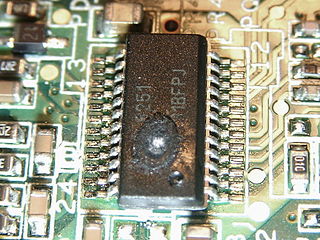
HASL or HAL is a type of finish used on printed circuit boards (PCBs).
Electroless nickel immersion gold (ENIG or ENi/IAu), also known as immersion gold (Au), chemical Ni/Au or soft gold, is a metal plating process used in the manufacture of printed circuit boards (PCBs), to avoid oxidation and improve the solderability of copper contacts and plated through-holes. It consists of an electroless nickel plating, covered with a thin layer of gold, which protects the nickel from oxidation. The gold is typically applied by quick immersion in a solution containing gold salts. Some of the nickel is oxidized to Ni2+ while the gold is reduced to metallic state. A variant of this process adds a thin layer of electroless palladium over the nickel, a process known by the acronym ENEPIG.
Immersion silver plating is a surface plating process that creates a thin layer of silver over copper objects. It consists in dipping the object briefly into a solution containing silver ions.
Electronic components have a wide range of failure modes. These can be classified in various ways, such as by time or cause. Failures can be caused by excess temperature, excess current or voltage, ionizing radiation, mechanical shock, stress or impact, and many other causes. In semiconductor devices, problems in the device package may cause failures due to contamination, mechanical stress of the device, or open or short circuits.
Ellington Electronics Technology Group 依頓電子科技股份有限公司 is one of the leading printed circuit board (PCB) manufacturers in China. It is a Hong Kong–based company which is listed on the Shanghai Stock Exchange on 1 July 2014. In Year 2018, the company was ranked Top 10 in China and 41st in the world by revenue.

Galvanic corrosion is an electrochemical process in which one metal corrodes preferentially when it is in electrical contact with another, in the presence of an electrolyte. A similar galvanic reaction is exploited in primary cells to generate a useful electrical voltage to power portable devices. This phenomenon is named after Italian physician Luigi Galvani (1737–1798).
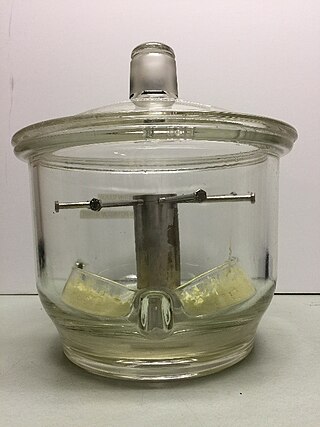
Flowers of sulfur (FOS) testing was developed to determine the porosity of metallic coatings susceptible to sulfur induced corrosion [see below ASTM B809-95(2018)]. Applicable substrates are silver, copper, copper alloys and any other metal or metal alloy with which sulfur will react. For porosity testing, coatings can be single or multiple layers of any metal that is not corroded and sealed by a self-limiting reaction in the reducing sulfur environment of the FOS test. The simplest recommended technique is to identify any porosity of the coating as revealed by the presence of surface spots. These surface spots form where the environmental sulfur has penetrated and reacted with the base metal, producing a metal sulfide. Chalcocite, copper (I) sulfide is dark-grey to black. Silver (I) sulfide is also grey-black.

Printed circuit board manufacturing is the process of manufacturing bare printed circuit boards (PCBs) and then populating them with electronic components. It involves the full assembly of a board into a functional circuit board.
References
- Tong, K. H., M. T. Ku, K. L. Hsu, Q. Tang, C. Y. Chan, and K. W. Yee. “The Evolution of Organic Solderability Preservative (OSP) Process in PCB Application.” 2013 8th International Microsystems, Packaging, Assembly and Circuits Technology Conference (IMPACT). Institute of Electrical & Electronics Engineers (IEEE), October 2013. doi:10.1109/impact.2013.6706620.
| | This industry-related article is a stub. You can help Wikipedia by expanding it. |