A transistor is a semiconductor device used to amplify or switch electronic signals and electrical power. It is composed of semiconductor material usually with at least three terminals for connection to an external circuit. A voltage or current applied to one pair of the transistor's terminals controls the current through another pair of terminals. Because the controlled (output) power can be higher than the controlling (input) power, a transistor can amplify a signal. Today, some transistors are packaged individually, but many more are found embedded in integrated circuits.
The junction gate field-effect transistor is one of the simplest types of field-effect transistor. JFETs are three-terminal semiconductor devices that can be used as electronically-controlled switches, amplifiers, or voltage-controlled resistors.
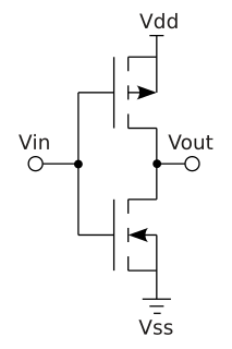
Complementary metal–oxide–semiconductor (CMOS), also known as complementary-symmetry metal–oxide–semiconductor (COS-MOS), is a type of MOSFET fabrication process that uses complementary and symmetrical pairs of p-type and n-type MOSFETs for logic functions. CMOS technology is used for constructing integrated circuits (ICs), including microprocessors, microcontrollers, memory chips, and other digital logic circuits. CMOS technology is also used for analog circuits such as image sensors, data converters, RF circuits, and highly integrated transceivers for many types of communication.
Transconductance, also infrequently called mutual conductance, is the electrical characteristic relating the current through the output of a device to the voltage across the input of a device. Conductance is the reciprocal of resistance.
A MESFET is a field-effect transistor semiconductor device similar to a JFET with a Schottky (metal-semiconductor) junction instead of a p-n junction for a gate.

For power semiconductor devices, the safe operating area (SOA) is defined as the voltage and current conditions over which the device can be expected to operate without self-damage.
The cascode is a two-stage amplifier that consists of a common-emitter stage feeding into a common-base stage.

A power MOSFET is a specific type of MOSFET designed to handle significant power levels.

One of several short-channel effects in MOSFET scaling, channel length modulation (CLM) is a shortening of the length of the inverted channel region with increase in drain bias for large drain biases. The result of CLM is an increase in current with drain bias and a reduction of output resistance. Channel length modulation occurs in all field effect transistors, not just MOSFETs.

A VMOS transistor is a type of MOSFET. VMOS is also used for describing the V-groove shape vertically cut into the substrate material. VMOS is an acronym for "vertical metal oxide semiconductor", or "V-groove MOS".
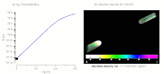
Capacitance–voltage profiling is a technique for characterizing semiconductor materials and devices. The applied voltage is varied, and the capacitance is measured and plotted as a function of voltage. The technique uses a metal–semiconductor junction or a p–n junction or a MOSFET to create a depletion region, a region which is empty of conducting electrons and holes, but may contain ionized donors and electrically active defects or traps. The depletion region with its ionized charges inside behaves like a capacitor. By varying the voltage applied to the junction it is possible to vary the depletion width. The dependence of the depletion width upon the applied voltage provides information on the semiconductor's internal characteristics, such as its doping profile and electrically active defect densities., Measurements may be done at DC, or using both DC and a small-signal AC signal, or using a large-signal transient voltage.
Negative-bias temperature instability (NBTI) is a key reliability issue in MOSFETs. NBTI manifests as an increase in the threshold voltage and consequent decrease in drain current and transconductance of a MOSFET. The degradation is often approximated by a power-law dependence on time. It is of immediate concern in p-channel MOS devices (pMOS), since they almost always operate with negative gate-to-source voltage; however, the very same mechanism also affects nMOS transistors when biased in the accumulation regime, i.e. with a negative bias applied to the gate.
Hot carrier injection (HCI) is a phenomenon in solid-state electronic devices where an electron or a “hole” gains sufficient kinetic energy to overcome a potential barrier necessary to break an interface state. The term "hot" refers to the effective temperature used to model carrier density, not to the overall temperature of the device. Since the charge carriers can become trapped in the gate dielectric of a MOS transistor, the switching characteristics of the transistor can be permanently changed. Hot-carrier injection is one of the mechanisms that adversely affects the reliability of semiconductors of solid-state devices.
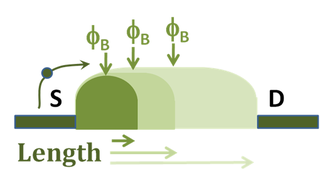
Drain-induced barrier lowering (DIBL) is a short-channel effect in MOSFETs referring originally to a reduction of threshold voltage of the transistor at higher drain voltages. In a classic planar field-effect transistor with a long channel, the bottleneck in channel formation occurs far enough from the drain contact that it is electrostatically shielded from the drain by the combination of the substrate and gate, and so classically the threshold voltage was independent of drain voltage. In short-channel devices this is no longer true: The drain is close enough to gate the channel, and so a high drain voltage can open the bottleneck and turn on the transistor prematurely.
In electronics, a native transistor is a variety of the MOS field-effect transistor that is intermediate between enhancement and depletion modes. Most common is the n-channel native transistor.
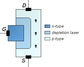
In field effect transistors (FETs), depletion mode and enhancement mode are two major transistor types, corresponding to whether the transistor is in an ON state or an OFF state at zero gate–source voltage.
Polysilicon depletion effect is the phenomenon in which unwanted variation of threshold voltage of the MOSFET devices using polysilicon as gate material is observed, leading to unpredicted behavior of the electronic circuit. Polycrystalline silicon, also called polysilicon, is a material consisting of small silicon crystals. It differs from single-crystal silicon, used for electronics and solar cells, and from amorphous silicon, used for thin film devices and solar cells.

The field-effect transistor (FET) is an electronic device which uses an electric field to control the flow of current. FETs are devices with three terminals: source, gate, and drain. FETs control the flow of current by the application of a voltage to the gate, which in turn alters the conductivity between the drain and source.