Process variation (semiconductor)

Last updated

Process variation is the naturally occurring variation in the attributes of transistors (length, widths, oxide thickness) when integrated circuits are fabricated. [1] The amount of process variation becomes particularly pronounced at smaller process nodes (<65 nm) as the variation becomes a larger percentage of the full length or width of the device and as feature sizes approach the fundamental dimensions such as the size of atoms and the wavelength of usable light for patterning lithography masks.

Integrated circuit electronic circuit manufactured by lithography; set of electronic circuits on one small flat piece (or "chip") of semiconductor material, normally silicon

An integrated circuit or monolithic integrated circuit is a set of electronic circuits on one small flat piece of semiconductor material that is normally silicon. The integration of large numbers of tiny transistors into a small chip results in circuits that are orders of magnitude smaller, faster, and less expensive than those constructed of discrete electronic components. The IC's mass production capability, reliability, and building-block approach to circuit design has ensured the rapid adoption of standardized ICs in place of designs using discrete transistors. ICs are now used in virtually all electronic equipment and have revolutionized the world of electronics. Computers, mobile phones, and other digital home appliances are now inextricable parts of the structure of modern societies, made possible by the small size and low cost of ICs.

Semiconductor device fabrication process used to create the integrated circuits that are present in everyday electrical and electronic devices

Semiconductor device fabrication is the process used to create the integrated circuits that are present in everyday electrical and electronic devices. It is a multiple-step sequence of photolithographic and chemical processing steps during which electronic circuits are gradually created on a wafer made of pure semiconducting material. Silicon is almost always used, but various compound semiconductors are used for specialized applications.

The term die shrink refers to a simple semiconductor scaling of semiconductor devices, mainly transistors. The act of shrinking a die is to create a somewhat identical circuit using a more advanced fabrication process, usually involving an advance of lithographic node. This reduces overall costs for a chip company, as the absence of major architectural changes to the processor lowers research and development costs, while at the same time allowing more processor dies to be manufactured on the same piece of silicon wafer, resulting in less cost per product sold.

Contents

Process variation causes measurable and predictable variance in the output performance of all circuits but particularly analog circuits due to mismatch. [2] If the variance causes the measured or simulated performance of a particular output metric (bandwidth, gain, rise time, etc.) to fall below or rise above the specification for the particular circuit or device, it reduces the overall yield for that set of devices.

History

The first mention of variation in semiconductors was by William Shockley, the co-inventor of the transistor, in his 1961 analysis of junction breakdown. [3]

William Shockley American physicist and inventor

William Bradford Shockley Jr. was an American physicist and inventor. Shockley was the manager of a research group at Bell Labs that included John Bardeen and Walter Brattain. The three scientists were jointly awarded the 1956 Nobel Prize in Physics for "their researches on semiconductors and their discovery of the transistor effect".

An analysis of systematic variation was performed by Schemmert and Zimmer in 1974 with their paper on threshold-voltage sensitivity. [4] This research looked into the effect that the oxide thickness and implantation energy had on the threshold voltage of MOS devices.

Threshold voltage Minimum source-to-gate voltage for a field effect transistor to be conducting from source to drain

The threshold voltage, commonly abbreviated as Vth, of a field-effect transistor (FET) is the minimum gate-to-source voltage VGS (th) that is needed to create a conducting path between the source and drain terminals. It is an important scaling factor to maintain power efficiency.

sources of variations 1) gate oxide thickness 2) random dopant fluctuations 3) Device Geometry, Lithography in nanometer region

Characterization

Semiconductor foundries run analyses on the variability of attributes of transistors (length, width, oxide thickness, etc.) for each new process node. These measurements are recorded and provided to customers such as fabless semiconductor companies. This set of files are generally referred to as "model files" in the industry and are used by EDA tools for simulation of designs.

FEOL

Typically process models (example HSPICE ) include process corners based on Front End Of Line conditions. These often are centered at a typical or nominal point and will also contain Fast and Slow corners often separated into Ntype and Ptype corners that affect the non-linear active N+ / P+ devices in different ways. Examples are TT for nominal N+ and P+ transistors, FF for fast N+ and P+ transistors, FS for fast N+ and slow P+ transistors, etc.

In semiconductor manufacturing, a process corner is an example of a design-of-experiments (DoE) technique that refers to a variation of fabrication parameters used in applying an integrated circuit design to a semiconductor wafer. Process corners represent the extremes of these parameter variations within which a circuit that has been etched onto the wafer must function correctly. A circuit running on devices fabricated at these process corners may run slower or faster than specified and at lower or higher temperatures and voltages, but if the circuit does not function at all at any of these process extremes the design is considered to have inadequate design margin.

Front end of line

The front-end-of-line (FEOL) is the first portion of IC fabrication where the individual devices are patterned in the semiconductor. FEOL generally covers everything up to the deposition of metal interconnect layers.

BEOL

When modeling the parasitic wiring an orthogonal set of process corners is often supplied with the parasitic extraction deck. (Example STAR-RC extraction deck) These corners are usually listed as Typical/Nominal for the target value and Cbest / Cworst corners for the variations in: conductor thickness, conductor width, and conductor oxide thickness that result in the Least / Most capacitance on the wiring. Often an additional corner called RCbest and RCworst is supplied that picks the conductor parameters that result in the Best (lowest) and worst (highest) wiring resistance for thickness and width, and then adds the oxide thicksness that adds the Best (lowest) and Worst (highest) capacitance due to the oxide thickness as this value is not directly correlated to wiring resistance.

Workarounds & Solutions

Statistical Analysis

Designers using this approach run from tens to thousands of simulations to analyze how the outputs of the circuit will behave according to the measured variability of the transistors for that particular process. The measured criteria for transistors are recorded in model files given to designers for simulating their circuits before simulation.

The most basic approach used by designers is increasing the size of devices which are sensitive to mismatch.

Topology Optimization

This is used to reduce variation due to polishing, etc. [5]

Patterning Techniques

To reduce roughness of line edges, advanced lithography techniques are used.

See also

Related Research Articles

MOSFET transistor used for amplifying or switching electronic signals

The metal–oxide–semiconductor field-effect transistor is a type of field-effect transistor (FET), most commonly fabricated by the controlled oxidation of silicon. It has an insulated gate, whose voltage determines the conductivity of the device. This ability to change conductivity with the amount of applied voltage can be used for amplifying or switching electronic signals. A metal-insulator-semiconductor field-effect transistor or MISFET is a term almost synonymous with MOSFET. Another synonym is IGFET for insulated-gate field-effect transistor.

CMOS technology for constructing integrated circuits

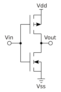
Complementary metal–oxide–semiconductor (CMOS) is a technology for constructing integrated circuits. CMOS technology is used in microprocessors, microcontrollers, static RAM, and other digital logic circuits. CMOS technology is also used for several analog circuits such as image sensors, data converters, and highly integrated transceivers for many types of communication. Frank Wanlass invented CMOS in 1963 while at Fairchild Semiconductor and was granted US patent 3,356,858 in 1967.

Silicon on insulator (SOI) technology refers to the use of a layered silicon–insulator–silicon substrate in place of conventional silicon substrates in semiconductor manufacturing, especially microelectronics, to reduce parasitic device capacitance, thereby improving performance. SOI-based devices differ from conventional silicon-built devices in that the silicon junction is above an electrical insulator, typically silicon dioxide or sapphire. The choice of insulator depends largely on intended application, with sapphire being used for high-performance radio frequency (RF) and radiation-sensitive applications, and silicon dioxide for diminished short channel effects in microelectronics devices. The insulating layer and topmost silicon layer also vary widely with application.

In computer engineering, a logic family may refer to one of two related concepts. A logic family of monolithic digital integrated circuit devices is a group of electronic logic gates constructed using one of several different designs, usually with compatible logic levels and power supply characteristics within a family. Many logic families were produced as individual components, each containing one or a few related basic logical functions, which could be used as "building-blocks" to create systems or as so-called "glue" to interconnect more complex integrated circuits. A "logic family" may also refer to a set of techniques used to implement logic within VLSI integrated circuits such as central processors, memories, or other complex functions. Some such logic families use static techniques to minimize design complexity. Other such logic families, such as domino logic, use clocked dynamic techniques to minimize size, power consumption and delay.

Planar process

The planar process is a manufacturing process used in the semiconductor industry to build individual components of a transistor, and in turn, connect those transistors together. It is the primary process by which modern integrated circuits are built. The process was developed by Jean Hoerni, one of the "traitorous eight", while working at Fairchild Semiconductor, with a first patent issued 1959.

Small-signal modeling is a common analysis technique in electronics engineering which is used to approximate the behavior of electronic circuits containing nonlinear devices with linear equations. It is applicable to electronic circuits in which the AC signals, the time-varying currents and voltages in the circuit, have a small magnitude compared to the DC bias currents and voltages. A small-signal model is an AC equivalent circuit in which the nonlinear circuit elements are replaced by linear elements whose values are given by the first-order (linear) approximation of their characteristic curve near the bias point.

The 65-nanometerprocess is advanced lithographic node used in volume CMOS semiconductor fabrication. Printed linewidths can reach as low as 25 nm on a nominally 65 nm process, while the pitch between two lines may be greater than 130 nm. For comparison, cellular ribosomes are about 20 nm end-to-end. A crystal of bulk silicon has a lattice constant of 0.543 nm, so such transistors are on the order of 100 atoms across. By September 2007, Intel, AMD, IBM, UMC, Chartered and TSMC were producing 65 nm chips.

The term high-κ dielectric refers to a material with a high dielectric constant κ. High-κ dielectrics are used in semiconductor manufacturing processes where they are usually used to replace a silicon dioxide gate dielectric or another dielectric layer of a device. The implementation of high-κ gate dielectrics is one of several strategies developed to allow further miniaturization of microelectronic components, colloquially referred to as extending Moore's Law.

Power MOSFET power MOS field-effect transistor

A power MOSFET is a specific type of metal oxide semiconductor field-effect transistor (MOSFET) designed to handle significant power levels.

Depletion-load NMOS logic form of nMOS logic family

In integrated circuits, depletion-load NMOS is a form of digital logic family that uses only a single power supply voltage, unlike earlier nMOS logic families that needed more than one different power supply voltage. Although manufacturing these integrated circuits required additional processing steps, improved switching speed and the elimination of the extra power supply made this logic family the preferred choice for many microprocessors and other logic elements.

Transistors are simple devices with complicated behavior. In order to ensure the reliable operation of circuits employing transistors, it is necessary to scientifically model the physical phenomena observed in their operation using transistor models. There exists a variety of different models that range in complexity and in purpose. Transistor models divide into two major groups: models for device design and models for circuit design.

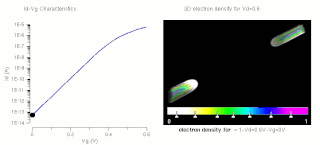
Capacitance–voltage profiling is a technique for characterizing semiconductor materials and devices. The applied voltage is varied, and the capacitance is measured and plotted as a function of voltage. The technique uses a metal–semiconductor junction or a p–n junction or a MOSFET to create a depletion region, a region which is empty of conducting electrons and holes, but may contain ionized donors and electrically active defects or traps. The depletion region with its ionized charges inside behaves like a capacitor. By varying the voltage applied to the junction it is possible to vary the depletion width. The dependence of the depletion width upon the applied voltage provides information on the semiconductor's internal characteristics, such as its doping profile and electrically active defect densities., Measurements may be done at DC, or using both DC and a small-signal AC signal, or using a large-signal transient voltage.

Shallow trench isolation integrated circuit

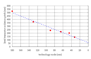
Shallow trench isolation (STI), also known as box isolation technique, is an integrated circuit feature which prevents electric current leakage between adjacent semiconductor device components. STI is generally used on CMOS process technology nodes of 250 nanometers and smaller. Older CMOS technologies and non-MOS technologies commonly use isolation based on LOCOS.

In electronics, a self-aligned gate is a transistor manufacturing feature whereby a refractory gate electrode region of a MOSFET transistor is used as a mask for the doping of the source and drain regions. This technique ensures that the gate will slightly overlap the edges of the source and drain.

Multi-threshold CMOS (MTCMOS) is a variation of CMOS chip technology which has transistors with multiple threshold voltages (Vth) in order to optimize delay or power. The Vth of a MOSFET is the gate voltage where an inversion layer forms at the interface between the insulating layer (oxide) and the substrate (body) of the transistor. Low Vth devices switch faster, and are therefore useful on critical delay paths to minimize clock periods. The penalty is that low Vth devices have substantially higher static leakage power. High Vth devices are used on non-critical paths to reduce static leakage power without incurring a delay penalty. Typical high Vth devices reduce static leakage by 10 times compared with low Vth devices.

Polysilicon depletion effect is the phenomenon in which unwanted variation of threshold voltage of the MOSFET devices using polysilicon as gate material is observed, leading to unpredicted behavior of the electronic circuit. Polycrystalline silicon, also called polysilicon, is a material consisting of small silicon crystals. It differs from single-crystal silicon, used for electronics and solar cells, and from amorphous silicon, used for thin film devices and solar cells.

Field-effect transistor transistor that uses an electric field to control the electrical behaviour of the device. FETs are also known as unipolar transistors since they involve single-carrier-type operation

The field-effect transistor (FET) is an electronic device which uses an electric field to control the flow of current. FETs are 3-terminalled devices, having a source, gate, and drain terminal. FETs control the flow of current by the application of a voltage to the gate terminal, which in turn alters the conductivity between the drain and source terminals.

References

  1. "A Survey Of Architectural Techniques for Managing Process Variation", ACM Computing Surveys, 2015
  2. Patrick Drennan, "Understanding MOSFET Mismatch for Analog Design" IEEE Journal of Solid-State Circuits, Vol 38, No 3, March 2003
  3. W. Shockley, “Problems related to p-n junctions in silicon.” Solid-State Electronics, Volume 2, January 1961, pp. 35–67.
  4. W. Schemmert, G. Zimmer, "Threshold-voltage sensitivity of ion-implanted m.o.s.transistors due to process variations." Electronics Letters, Volume 10, Issue 9, May 2, 1974, pp. 151-152
  5. "Managing Process Variation in Intel's 45nm CMOS Technology." Intel Technology Journal, Volume 12, Issue 2 June 17, 2008 http://www.intel.com/technology/itj/2008/v12i2/3-managing/1-abstract.htm