
The Intel 486, officially named i486 and also known as 80486, is a microprocessor. It is a higher-performance follow-up to the Intel 386. The i486 was introduced in 1989. It represents the fourth generation of binary compatible CPUs following the 8086 of 1978, the Intel 80286 of 1982, and 1985's i386.

Celeron is a discontinued series of low-end IA-32 and x86-64 computer microprocessor models targeted at low-cost personal computers, manufactured by Intel. The first Celeron-branded CPU was introduced on April 15, 1998, and was based on the Pentium II.
Rambus DRAM (RDRAM), and its successors Concurrent Rambus DRAM (CRDRAM) and Direct Rambus DRAM (DRDRAM), are types of synchronous dynamic random-access memory (SDRAM) developed by Rambus from the 1990s through to the early 2000s. The third-generation of Rambus DRAM, DRDRAM was replaced by XDR DRAM. Rambus DRAM was developed for high-bandwidth applications and was positioned by Rambus as replacement for various types of contemporary memories, such as SDRAM.

Pentium 4 is a series of single-core CPUs for desktops, laptops and entry-level servers manufactured by Intel. The processors were shipped from November 20, 2000 until August 8, 2008. It was removed from the official price lists starting in 2010, being replaced by Pentium Dual-Core.

The Pentium III brand refers to Intel's 32-bit x86 desktop and mobile CPUs based on the sixth-generation P6 microarchitecture introduced on February 28, 1999. The brand's initial processors were very similar to the earlier Pentium II-branded processors. The most notable differences were the addition of the Streaming SIMD Extensions (SSE) instruction set, and the introduction of a controversial serial number embedded in the chip during manufacturing. The Pentium III is also a single-core processor.

The front-side bus (FSB) is a computer communication interface (bus) that was often used in Intel-chip-based computers during the 1990s and 2000s. The EV6 bus served the same function for competing AMD CPUs. Both typically carry data between the central processing unit (CPU) and a memory controller hub, known as the northbridge.

The Athlon 64 is a ninth-generation, AMD64-architecture microprocessor produced by Advanced Micro Devices (AMD), released on September 23, 2003. It is the third processor to bear the name Athlon, and the immediate successor to the Athlon XP. The Athlon 64 was the second processor to implement the AMD64 architecture and the first 64-bit processor targeted at the average consumer. Variants of the Athlon 64 have been produced for Socket 754, Socket 939, Socket 940, and Socket AM2. It was AMD's primary consumer CPU, and primarily competed with Intel's Pentium 4, especially the Prescott and Cedar Mill core revisions.

In computing, the clock rate or clock speed typically refers to the frequency at which the clock generator of a processor can generate pulses, which are used to synchronize the operations of its components, and is used as an indicator of the processor's speed. It is measured in the SI unit of frequency hertz (Hz).
The NetBurst microarchitecture, called P68 inside Intel, was the successor to the P6 microarchitecture in the x86 family of central processing units (CPUs) made by Intel. The first CPU to use this architecture was the Willamette-core Pentium 4, released on November 20, 2000 and the first of the Pentium 4 CPUs; all subsequent Pentium 4 and Pentium D variants have also been based on NetBurst. In mid-2001, Intel released the Foster core, which was also based on NetBurst, thus switching the Xeon CPUs to the new architecture as well. Pentium 4-based Celeron CPUs also use the NetBurst architecture.
Quad Data Rate (QDR) SRAM is a type of static RAM computer memory that can transfer up to four words of data in each clock cycle. Like Double Data-Rate (DDR) SDRAM, QDR SRAM transfers data on both rising and falling edges of the clock signal. The main purpose of this capability is to enable reads and writes to occur at high clock frequencies without the loss of bandwidth due to bus-turnaround cycles incurred in DDR SRAM. QDR SRAM uses two clocks, one for read data and one for write data and has separate read and write data buses, whereas DDR SRAM uses a single clock and has a single common data bus used for both reads and writes. This helps to eliminate problems caused by the propagation delay of the clock wiring, and allows the illusion of concurrent reads and writes.
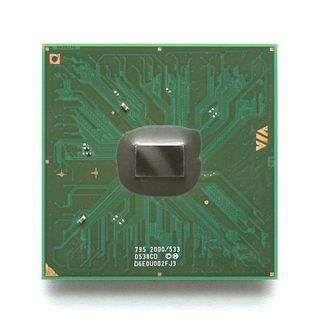
The VIA C7 is an x86 central processing unit designed by Centaur Technology and sold by VIA Technologies.

In computing, double data rate (DDR) describes a computer bus that transfers data on both the rising and falling edges of the clock signal and hence doubles the memory bandwidth by transferring data twice per clock cycle. This is also known as double pumped, dual-pumped, and double transition. The term toggle mode is used in the context of NAND flash memory.
Pentium D is a range of desktop 64-bit x86-64 processors based on the NetBurst microarchitecture, which is the dual-core variant of the Pentium 4 manufactured by Intel. Each CPU comprised two cores. The brand's first processor, codenamed Smithfield and manufactured on the 90 nm process, was released on May 25, 2005, followed by the 65 nm Presler nine months later. The core implementation on the 90 nm Smithfield and later 65 nm Presler are designed differently but are functionally the same. The 90 nm Smithfield contains a single die, with two adjoined but functionally separate CPU cores cut from the same wafer. The later 65 nm Presler utilized a multi-chip module package, where two discrete dies each containing a single core reside on the CPU substrate. Neither the 90 nm Smithfield nor the 65 nm Presler were capable of direct core to core communication, relying instead on the northbridge link to send information between the two cores.
The P6 microarchitecture is the sixth-generation Intel x86 microarchitecture, implemented by the Pentium Pro microprocessor that was introduced in November 1995. It is frequently referred to as i686. It was planned to be succeeded by the NetBurst microarchitecture used by the Pentium 4 in 2000, but was revived for the Pentium M line of microprocessors. The successor to the Pentium M variant of the P6 microarchitecture is the Core microarchitecture which in turn is also derived from P6.
The Intel Core microarchitecture is a multi-core processor microarchitecture launched by Intel in mid-2006. It is a major evolution over the Yonah, the previous iteration of the P6 microarchitecture series which started in 1995 with Pentium Pro. It also replaced the NetBurst microarchitecture, which suffered from high power consumption and heat intensity due to an inefficient pipeline designed for high clock rate. In early 2004 the new version of NetBurst (Prescott) needed very high power to reach the clocks it needed for competitive performance, making it unsuitable for the shift to dual/multi-core CPUs. On May 7, 2004 Intel confirmed the cancellation of the next NetBurst, Tejas and Jayhawk. Intel had been developing Merom, the 64-bit evolution of the Pentium M, since 2001, and decided to expand it to all market segments, replacing NetBurst in desktop computers and servers. It inherited from Pentium M the choice of a short and efficient pipeline, delivering superior performance despite not reaching the high clocks of NetBurst.
Double Data Rate 3 Synchronous Dynamic Random-Access Memory is a type of synchronous dynamic random-access memory (SDRAM) with a high bandwidth interface, and has been in use since 2007. It is the higher-speed successor to DDR and DDR2 and predecessor to DDR4 synchronous dynamic random-access memory (SDRAM) chips. DDR3 SDRAM is neither forward nor backward compatible with any earlier type of random-access memory (RAM) because of different signaling voltages, timings, and other factors.

In computing, the clock multiplier sets the ratio of an internal CPU clock rate to the externally supplied clock. This may be implemented with phase-locked loop (PLL) frequency multiplier circuitry. A CPU with a 10x multiplier will thus see 10 internal cycles for every external clock cycle. For example, a system with an external clock of 100 MHz and a 36x clock multiplier will have an internal CPU clock of 3.6 GHz. The external address and data buses of the CPU also use the external clock as a fundamental timing base; however, they could also employ a (small) multiple of this base frequency to transfer data faster.
Pumping, when referring to computer systems, is an informal term for transmitting a data signal more than one time per clock signal.

Conroe is the code name for many Intel processors sold as Core 2 Duo, Xeon, Pentium Dual-Core and Celeron. It was the first desktop processor to be based on the Core microarchitecture, replacing the NetBurst microarchitecture based Cedar Mill processor. It has product code 80557, which is shared with Allendale and Conroe-L that are very similar but have a smaller L2 cache. Conroe-L has only one processor core and a new CPUID model. The mobile version of Conroe is Merom, the dual-socket server version is Woodcrest, the quad-core desktop version is Kentsfield and the quad-core dual-socket version is Clovertown. Conroe was replaced by the 45 nm Wolfdale processor.

