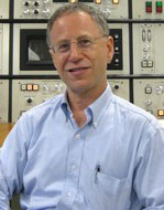
Richard D. Leapman | |
---|---|
Personal details | |
Born | December 6, 1950 |
Education | University of Cambridge |
Richard D. Leapman (born 6 December 1950) is an English physicist who is current scientific director of National Institute of Biomedical Imaging and Bioengineering (NIBIB), since October 2006 [1] and a chief of the laboratory of bioengineering and physical science. Leapman's research interests are in the development and application of quantitative electron microscopy and the application of novel nanoscale imaging methods to solve problems in structural and cellular biology.
Leapman has been active in developing the techniques of electron energy loss spectroscopy (EELS) and scanning transmission electron microscopy (STEM) to provide an unprecedented high spatial resolution for nanoanalysis of biological structures. Leapman has devised new methods for quantifying both elemental and chemical information obtained from inelastic electron scattering, a research area in which he has over one hundred publications. [2] Leapman has extended the techniques of energy filtered transmission electron microscopy (EFTEM) and STEM and combined them with a known technique of tomography to obtain three-dimensional structural and compositional information of cellular components.
Leapman obtained his Ph.D. in physics from the University of Cambridge, England. He serves on the editorial boards of the journal of microscopy and nanotechnology and on peer review panels.
An electron microscope is a microscope that uses a beam of electrons as a source of illumination. They use electron optics that are analogous to the glass lenses of an optical light microscope to control the electron beam, for instance focusing them to produce magnified images or electron diffraction patterns. As the wavelength of an electron can be up to 100,000 times smaller than that of visible light, electron microscopes have a much higher resolution of about 0.1 nm, which compares to about 200 nm for light microscopes. Electron microscope may refer to:
Microscopy is the technical field of using microscopes to view objects and areas of objects that cannot be seen with the naked eye. There are three well-known branches of microscopy: optical, electron, and scanning probe microscopy, along with the emerging field of X-ray microscopy.
A scanning electron microscope (SEM) is a type of electron microscope that produces images of a sample by scanning the surface with a focused beam of electrons. The electrons interact with atoms in the sample, producing various signals that contain information about the surface topography and composition of the sample. The electron beam is scanned in a raster scan pattern, and the position of the beam is combined with the intensity of the detected signal to produce an image. In the most common SEM mode, secondary electrons emitted by atoms excited by the electron beam are detected using a secondary electron detector. The number of secondary electrons that can be detected, and thus the signal intensity, depends, among other things, on specimen topography. Some SEMs can achieve resolutions better than 1 nanometer.
Transmission electron microscopy (TEM) is a microscopy technique in which a beam of electrons is transmitted through a specimen to form an image. The specimen is most often an ultrathin section less than 100 nm thick or a suspension on a grid. An image is formed from the interaction of the electrons with the sample as the beam is transmitted through the specimen. The image is then magnified and focused onto an imaging device, such as a fluorescent screen, a layer of photographic film, or a detector such as a scintillator attached to a charge-coupled device or a direct electron detector.
An X-ray microscope uses electromagnetic radiation in the X-ray band to produce magnified images of objects. Since X-rays penetrate most objects, there is no need to specially prepare them for X-ray microscopy observations.
A scanning transmission electron microscope (STEM) is a type of transmission electron microscope (TEM). Pronunciation is [stɛm] or [ɛsti:i:ɛm]. As with a conventional transmission electron microscope (CTEM), images are formed by electrons passing through a sufficiently thin specimen. However, unlike CTEM, in STEM the electron beam is focused to a fine spot which is then scanned over the sample in a raster illumination system constructed so that the sample is illuminated at each point with the beam parallel to the optical axis. The rastering of the beam across the sample makes STEM suitable for analytical techniques such as Z-contrast annular dark-field imaging, and spectroscopic mapping by energy dispersive X-ray (EDX) spectroscopy, or electron energy loss spectroscopy (EELS). These signals can be obtained simultaneously, allowing direct correlation of images and spectroscopic data.
Focused ion beam, also known as FIB, is a technique used particularly in the semiconductor industry, materials science and increasingly in the biological field for site-specific analysis, deposition, and ablation of materials. A FIB setup is a scientific instrument that resembles a scanning electron microscope (SEM). However, while the SEM uses a focused beam of electrons to image the sample in the chamber, a FIB setup uses a focused beam of ions instead. FIB can also be incorporated in a system with both electron and ion beam columns, allowing the same feature to be investigated using either of the beams. FIB should not be confused with using a beam of focused ions for direct write lithography. These are generally quite different systems where the material is modified by other mechanisms.
Cryogenic electron tomography (cryoET) is an imaging technique used to reconstruct high-resolution (~1–4 nm) three-dimensional volumes of samples, often biological macromolecules and cells. cryoET is a specialized application of transmission electron cryomicroscopy (CryoTEM) in which samples are imaged as they are tilted, resulting in a series of 2D images that can be combined to produce a 3D reconstruction, similar to a CT scan of the human body. In contrast to other electron tomography techniques, samples are imaged under cryogenic conditions. For cellular material, the structure is immobilized in non-crystalline, vitreous ice, allowing them to be imaged without dehydration or chemical fixation, which would otherwise disrupt or distort biological structures.
Annular dark-field imaging is a method of mapping samples in a scanning transmission electron microscope (STEM). These images are formed by collecting scattered electrons with an annular dark-field detector.
A scanning acoustic microscope (SAM) is a device which uses focused sound to investigate, measure, or image an object. It is commonly used in failure analysis and non-destructive evaluation. It also has applications in biological and medical research. The semiconductor industry has found the SAM useful in detecting voids, cracks, and delaminations within microelectronic packages.
Chemical imaging is the analytical capability to create a visual image of components distribution from simultaneous measurement of spectra and spatial, time information. Hyperspectral imaging measures contiguous spectral bands, as opposed to multispectral imaging which measures spaced spectral bands.
Electron tomography (ET) is a tomography technique for obtaining detailed 3D structures of sub-cellular, macro-molecular, or materials specimens. Electron tomography is an extension of traditional transmission electron microscopy and uses a transmission electron microscope to collect the data. In the process, a beam of electrons is passed through the sample at incremental degrees of rotation around the center of the target sample. This information is collected and used to assemble a three-dimensional image of the target. For biological applications, the typical resolution of ET systems are in the 5–20 nm range, suitable for examining supra-molecular multi-protein structures, although not the secondary and tertiary structure of an individual protein or polypeptide. Recently, atomic resolution in 3D electron tomography reconstructions has been demonstrated.
Optical sectioning is the process by which a suitably designed microscope can produce clear images of focal planes deep within a thick sample. This is used to reduce the need for thin sectioning using instruments such as the microtome. Many different techniques for optical sectioning are used and several microscopy techniques are specifically designed to improve the quality of optical sectioning.
The Ernst Ruska-Centre for Microscopy and Spectroscopy with Electrons (ER-C) is an institute located on the campus of Forschungszentrum Jülich belonging to the Helmholtz Association of German Research Centres. It comprises three divisions: ER-C-1 “Physics of Nanoscale systems”, ER-C-2 “Materials Science and Technology” and ER-C-3 “Structural Biology”.
Ondrej L. Krivanek is a Czech/British physicist resident in the United States, and a leading developer of electron-optical instrumentation. He won the Kavli Prize for Nanoscience in 2020 for his substantial innovations in atomic resolution electron microscopy.
The following outline is provided as an overview of and topical guide to biophysics:
Liquid-phase electron microscopy refers to a class of methods for imaging specimens in liquid with nanometer spatial resolution using electron microscopy. LP-EM overcomes the key limitation of electron microscopy: since the electron optics requires a high vacuum, the sample must be stable in a vacuum environment. Many types of specimens relevant to biology, materials science, chemistry, geology, and physics, however, change their properties when placed in a vacuum.
SOLARIS is the only synchrotron in Central-Eastern Europe. Built in Poland in 2015, under the auspices of the Jagiellonian University, it is located on the Campus of the 600th Anniversary of the Jagiellonian University Revival, in the southern part of Kraków. It is the central facility of the National Synchrotron Radiation Centre SOLARIS.
Convergent beam electron diffraction (CBED) is an electron diffraction technique where a convergent or divergent beam of electrons is used to study materials.
4D scanning transmission electron microscopy is a subset of scanning transmission electron microscopy (STEM) which utilizes a pixelated electron detector to capture a convergent beam electron diffraction (CBED) pattern at each scan location. This technique captures a 2 dimensional reciprocal space image associated with each scan point as the beam rasters across a 2 dimensional region in real space, hence the name 4D STEM. Its development was enabled by evolution in STEM detectors and improvements computational power. The technique has applications in visual diffraction imaging, phase orientation and strain mapping, phase contrast analysis, among others.