
Semiconductor device fabrication is the process used to manufacture semiconductor devices, typically integrated circuits (ICs) such as microprocessors, microcontrollers, and memories. It is a multiple-step photolithographic and physico-chemical process during which electronic circuits are gradually created on a wafer, typically made of pure single-crystal semiconducting material. Silicon is almost always used, but various compound semiconductors are used for specialized applications.
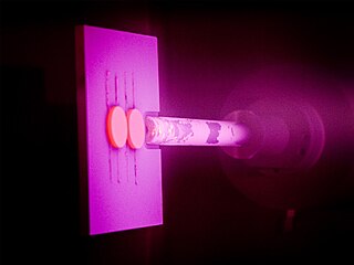
In physics, sputtering is a phenomenon in which microscopic particles of a solid material are ejected from its surface, after the material is itself bombarded by energetic particles of a plasma or gas. It occurs naturally in outer space, and can be an unwelcome source of wear in precision components. However, the fact that it can be made to act on extremely fine layers of material is utilised in science and industry—there, it is used to perform precise etching, carry out analytical techniques, and deposit thin film layers in the manufacture of optical coatings, semiconductor devices and nanotechnology products. It is a physical vapor deposition technique.
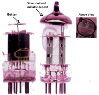
A getter is a deposit of reactive material that is placed inside a vacuum system to complete and maintain the vacuum. When gas molecules strike the getter material, they combine with it chemically or by adsorption. Thus the getter removes small amounts of gas from the evacuated space. The getter is usually a coating applied to a surface within the evacuated chamber.
A thin film is a layer of materials ranging from fractions of a nanometer (monolayer) to several micrometers in thickness. The controlled synthesis of materials as thin films is a fundamental step in many applications. A familiar example is the household mirror, which typically has a thin metal coating on the back of a sheet of glass to form a reflective interface. The process of silvering was once commonly used to produce mirrors, while more recently the metal layer is deposited using techniques such as sputtering. Advances in thin film deposition techniques during the 20th century have enabled a wide range of technological breakthroughs in areas such as magnetic recording media, electronic semiconductor devices, integrated passive devices, light-emitting diodes, optical coatings, hard coatings on cutting tools, and for both energy generation and storage. It is also being applied to pharmaceuticals, via thin-film drug delivery. A stack of thin films is called a multilayer.

A coating is a covering that is applied to the surface of an object, or substrate. The purpose of applying the coating may be decorative, functional, or both. Coatings may be applied as liquids, gases or solids e.g. powder coatings.

Silvering is the chemical process of coating a non-conductive substrate such as glass with a reflective substance, to produce a mirror. While the metal is often silver, the term is used for the application of any reflective metal.
Cathodic arc deposition or Arc-PVD is a physical vapor deposition technique in which an electric arc is used to vaporize material from a cathode target. The vaporized material then condenses on a substrate, forming a thin film. The technique can be used to deposit metallic, ceramic, and composite films.

Ion plating (IP) is a physical vapor deposition (PVD) process that is sometimes called ion assisted deposition (IAD) or ion vapor deposition (IVD) and is a modified version of vacuum deposition. Ion plating uses concurrent or periodic bombardment of the substrate, and deposits film by atomic-sized energetic particles called ions. Bombardment prior to deposition is used to sputter clean the substrate surface. During deposition the bombardment is used to modify and control the properties of the depositing film. It is important that the bombardment be continuous between the cleaning and the deposition portions of the process to maintain an atomically clean interface. If this interface is not properly cleaned, then it can result into a weaker coating or poor adhesion.
Plasma etching is a form of plasma processing used to fabricate integrated circuits. It involves a high-speed stream of glow discharge (plasma) of an appropriate gas mixture being shot at a sample. The plasma source, known as etch species, can be either charged (ions) or neutral. During the process, the plasma generates volatile etch products at room temperature from the chemical reactions between the elements of the material etched and the reactive species generated by the plasma. Eventually the atoms of the shot element embed themselves at or just below the surface of the target, thus modifying the physical properties of the target.
Electron-beam physical vapor deposition, or EBPVD, is a form of physical vapor deposition in which a target anode is bombarded with an electron beam given off by a charged tungsten filament under high vacuum. The electron beam causes atoms from the target to transform into the gaseous phase. These atoms then precipitate into solid form, coating everything in the vacuum chamber with a thin layer of the anode material.
Vacuum deposition is a group of processes used to deposit layers of material atom-by-atom or molecule-by-molecule on a solid surface. These processes operate at pressures well below atmospheric pressure. The deposited layers can range from a thickness of one atom up to millimeters, forming freestanding structures. Multiple layers of different materials can be used, for example to form optical coatings. The process can be qualified based on the vapor source; physical vapor deposition uses a liquid or solid source and chemical vapor deposition uses a chemical vapor.
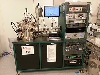
Physical vapor deposition (PVD), sometimes called physical vapor transport (PVT), describes a variety of vacuum deposition methods which can be used to produce thin films and coatings on substrates including metals, ceramics, glass, and polymers. PVD is characterized by a process in which the material transitions from a condensed phase to a vapor phase and then back to a thin film condensed phase. The most common PVD processes are sputtering and evaporation. PVD is used in the manufacturing of items which require thin films for optical, mechanical, electrical, acoustic or chemical functions. Examples include semiconductor devices such as thin-film solar cells, microelectromechanical devices such as thin film bulk acoustic resonator, aluminized PET film for food packaging and balloons, and titanium nitride coated cutting tools for metalworking. Besides PVD tools for fabrication, special smaller tools used mainly for scientific purposes have been developed.

Evaporation is a common method of thin-film deposition. The source material is evaporated in a vacuum. The vacuum allows vapor particles to travel directly to the target object (substrate), where they condense back to a solid state. Evaporation is used in microfabrication, and to make macro-scale products such as metallized plastic film.

Sputter deposition is a physical vapor deposition (PVD) method of thin film deposition by the phenomenon of sputtering. This involves ejecting material from a "target" that is a source onto a "substrate" such as a silicon wafer.
High-power impulse magnetron sputtering is a method for physical vapor deposition of thin films which is based on magnetron sputter deposition. HIPIMS utilises extremely high power densities of the order of kW⋅cm−2 in short pulses (impulses) of tens of microseconds at low duty cycle of < 10%. Distinguishing features of HIPIMS are a high degree of ionisation of the sputtered metal and a high rate of molecular gas dissociation which result in high density of deposited films. The ionization and dissociation degree increase according to the peak cathode power. The limit is determined by the transition of the discharge from glow to arc phase. The peak power and the duty cycle are selected so as to maintain an average cathode power similar to conventional sputtering (1–10 W⋅cm−2).
AVS: Science and Technology of Materials, Interfaces, and Processing is a not-for-profit learned society founded in 1953 focused on disciplines related to materials, interfaces, and processing. AVS has approximately 4500 members worldwide from academia, governmental laboratories and industry.
Plasma polymerization uses plasma sources to generate a gas discharge that provides energy to activate or fragment gaseous or liquid monomer, often containing a vinyl group, in order to initiate polymerization. Polymers formed from this technique are generally highly branched and highly cross-linked, and adhere to solid surfaces well. The biggest advantage to this process is that polymers can be directly attached to a desired surface while the chains are growing, which reduces steps necessary for other coating processes such as grafting. This is very useful for pinhole-free coatings of 100 picometers to 1-micrometer thickness with solvent insoluble polymers.

Ivan Georgiev Petrov is a Bulgarian-American physicist specializing in thin films, surface science, and methods of characterization of materials. His research and scientific contributions have been described as having an "enormous impact on the hard-coatings community". Petrov was the president of the American Vacuum Society for 2015.
Jeffrey Elam is a Distinguished Fellow, Senior Chemist and Group Leader in the Applied Materials Division at the U.S. Department of Energy's Argonne National Laboratory. He leads Argonne's atomic layer deposition (ALD) research program, where he directs research and development and commercialization of thin film coating technologies for energy applications.
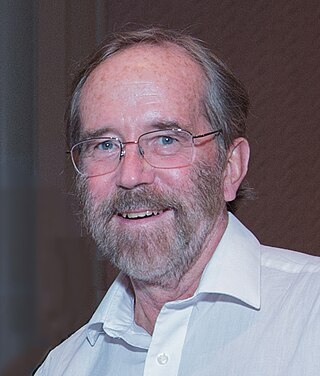
Joseph "Joe" E. Greene, known in his professional writing as J. E. Greene was an American materials scientist, specializing in thin films, crystal growth, surface science, and advanced surface engineering. His research and scientific contributions in these areas have been described as "pioneering" and "seminal" and that his work "revolutionized the hard-coating industry".