
An integrated circuit (IC), also known as a microchip or simply chip, is a small electronic device made up of multiple interconnected electronic components such as transistors, resistors, and capacitors. These components are etched onto a small piece of semiconductor material, usually silicon. Integrated circuits are used in a wide range of electronic devices, including computers, smartphones, and televisions, to perform various functions such as processing and storing information. They have greatly impacted the field of electronics by enabling device miniaturization and enhanced functionality.

A printed circuit board (PCB), also called printed wiring board (PWB), is a laminated sandwich structure of conductive and insulating layers, each with a pattern of traces, planes and other features etched from one or more sheet layers of copper laminated onto or between sheet layers of a non-conductive substrate. PCBs are used to connect or "wire" components to one another in an electronic circuit. Electrical components may be fixed to conductive pads on the outer layers, generally by soldering, which both electrically connects and mechanically fastens the components to the board. Another manufacturing process adds vias, metal-lined drilled holes that enable electrical interconnections between conductive layers, to boards with more than a single side.

Flexible electronics, also known as flex circuits, is a technology for assembling electronic circuits by mounting electronic components on flexible plastic substrates, such as polyimide, PEEK or transparent conductive polyester film. Additionally, flex circuits can be screen printed silver circuits on polyester. Flexible electronic assemblies may be manufactured using identical components used for rigid printed circuit boards, allowing the board to conform to a desired shape, or to flex during its use.

Flip chip, also known as controlled collapse chip connection or its abbreviation, C4, is a method for interconnecting dies such as semiconductor devices, IC chips, integrated passive devices and microelectromechanical systems (MEMS), to external circuitry with solder bumps that have been deposited onto the chip pads. The technique was developed by General Electric's Light Military Electronics Department, Utica, New York. The solder bumps are deposited on the chip pads on the top side of the wafer during the final wafer processing step. In order to mount the chip to external circuitry, it is flipped over so that its top side faces down, and aligned so that its pads align with matching pads on the external circuit, and then the solder is reflowed to complete the interconnect. This is in contrast to wire bonding, in which the chip is mounted upright and fine wires are welded onto the chip pads and lead frame contacts to interconnect the chip pads to external circuitry.

Integrated circuit packaging is the final stage of semiconductor device fabrication, in which the die is encapsulated in a supporting case that prevents physical damage and corrosion. The case, known as a "package", supports the electrical contacts which connect the device to a circuit board.
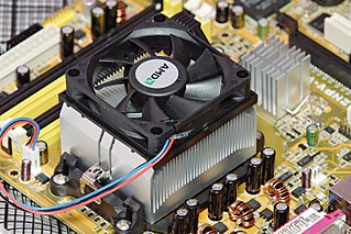
Computer cooling is required to remove the waste heat produced by computer components, to keep components within permissible operating temperature limits. Components that are susceptible to temporary malfunction or permanent failure if overheated include integrated circuits such as central processing units (CPUs), chipsets, graphics cards, hard disk drives, and solid state drives.

A via is an electrical connection between two or more metal layers of a printed circuit boards (PCB) or integrated circuit. Essentially a via is a small drilled hole that goes through two or more adjacent layers; the hole is plated with metal that forms an electrical connection through the insulating layers.

All electronic devices and circuitry generate excess heat and thus require thermal management to improve reliability and prevent premature failure. The amount of heat output is equal to the power input, if there are no other energy interactions. There are several techniques for cooling including various styles of heat sinks, thermoelectric coolers, forced air systems and fans, heat pipes, and others. In cases of extreme low environmental temperatures, it may actually be necessary to heat the electronic components to achieve satisfactory operation.
The role of the substrate in power electronics is to provide the interconnections to form an electric circuit, and to cool the components. Compared to materials and techniques used in lower power microelectronics, these substrates must carry higher currents and provide a higher voltage isolation. They also must operate over a wide temperature range.

Flat no-leads packages such as quad-flat no-leads (QFN) and dual-flat no-leads (DFN) physically and electrically connect integrated circuits to printed circuit boards. Flat no-leads, also known as micro leadframe (MLF) and SON, is a surface-mount technology, one of several package technologies that connect ICs to the surfaces of PCBs without through-holes. Flat no-lead is a near chip scale plastic encapsulated package made with a planar copper lead frame substrate. Perimeter lands on the package bottom provide electrical connections to the PCB. Flat no-lead packages usually, but not always, include an exposed thermally conductive pad to improve heat transfer out of the IC. Heat transfer can be further facilitated by metal vias in the thermal pad. The QFN package is similar to the quad-flat package (QFP), and a ball grid array (BGA).
Electronic packaging is the design and production of enclosures for electronic devices ranging from individual semiconductor devices up to complete systems such as a mainframe computer. Packaging of an electronic system must consider protection from mechanical damage, cooling, radio frequency noise emission and electrostatic discharge. Product safety standards may dictate particular features of a consumer product, for example, external case temperature or grounding of exposed metal parts. Prototypes and industrial equipment made in small quantities may use standardized commercially available enclosures such as card cages or prefabricated boxes. Mass-market consumer devices may have highly specialized packaging to increase consumer appeal. Electronic packaging is a major discipline within the field of mechanical engineering.

Hot stamping or foil stamping is a printing method of relief printing in which pre-dried ink or foils are transferred to a surface at high temperatures. The method has diversified since its rise to prominence in the 19th century to include a variety of processes. After the 1970s, hot stamping became one of the most important methods of decoration on the surface of plastic products.
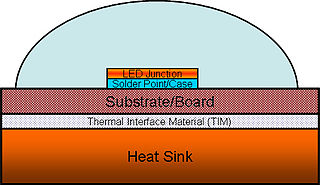
High power light-emitting diodes (LEDs) can use 350 milliwatts or more in a single LED. Most of the electricity in an LED becomes heat rather than light. If this heat is not removed, the LEDs run at high temperatures, which not only lowers their efficiency, but also makes the LED less reliable. Thus, thermal management of high power LEDs is a crucial area of research and development. It is necessary to limit both the junction and the phosphor particles temperatures to a value that will guarantee the desired LED lifetime.

A thermal copper pillar bump, also known as a "thermal bump", is a thermoelectric device made from thin-film thermoelectric material embedded in flip chip interconnects for use in electronics and optoelectronic packaging, including: flip chip packaging of CPU and GPU integrated circuits (chips), laser diodes, and semiconductor optical amplifiers (SOA). Unlike conventional solder bumps that provide an electrical path and a mechanical connection to the package, thermal bumps act as solid-state heat pumps and add thermal management functionality locally on the surface of a chip or to another electrical component. The diameter of a thermal bump is 238 μm and 60 μm high.
Microvias are used as the interconnects between layers in high density interconnect (HDI) substrates and printed circuit boards (PCBs) to accommodate the high input/output (I/O) density of advanced packages.
A molded interconnect device (MID) is an injection-molded thermoplastic part with integrated electronic circuit traces. The use of high temperature thermoplastics and their structured metallization opens a new dimension of circuit carrier design to the electronics industry. This technology combines plastic substrate/housing with circuitry into a single part by selective metallization.
AlSiC, pronounced "alsick", is a metal matrix composite consisting of aluminium matrix with silicon carbide particles. It has high thermal conductivity, and its thermal expansion can be adjusted to match other materials, e.g. silicon and gallium arsenide chips and various ceramics. It is chiefly used in microelectronics as substrate for power semiconductor devices and high density multi-chip modules, where it aids with removal of waste heat.
Electronic components have a wide range of failure modes. These can be classified in various ways, such as by time or cause. Failures can be caused by excess temperature, excess current or voltage, ionizing radiation, mechanical shock, stress or impact, and many other causes. In semiconductor devices, problems in the device package may cause failures due to contamination, mechanical stress of the device, or open or short circuits.

Co-fired ceramic devices are monolithic, ceramic microelectronic devices where the entire ceramic support structure and any conductive, resistive, and dielectric materials are fired in a kiln at the same time. Typical devices include capacitors, inductors, resistors, transformers, and hybrid circuits. The technology is also used for robust assembly and packaging of electronic components multi-layer packaging in the electronics industry, such as military electronics, MEMS, microprocessor and RF applications.

Printed circuit board manufacturing is the process of manufacturing bare printed circuit boards (PCBs) and then populating them with electronic components. It involves the full assembly of a board into a functional circuit board.