Related Research Articles

Celeron is a discontinued series of low-end IA-32 and x86-64 computer microprocessor models targeted at low-cost personal computers, manufactured by Intel. The first Celeron-branded CPU was introduced on April 15, 1998, and was based on the Pentium II.

Pentium 4 is a series of single-core CPUs for desktops, laptops and entry-level servers manufactured by Intel. The processors were shipped from November 20, 2000 until August 8, 2008. It was removed from the official price lists starting in 2010, being replaced by Pentium Dual-Core.

The Pentium III brand refers to Intel's 32-bit x86 desktop and mobile CPUs based on the sixth-generation P6 microarchitecture introduced on February 28, 1999. The brand's initial processors were very similar to the earlier Pentium II-branded processors. The most notable differences were the addition of the Streaming SIMD Extensions (SSE) instruction set, and the introduction of a controversial serial number embedded in the chip during manufacturing.
The Pentium OverDrive was a microprocessor marketing brand name used by Intel, to cover a variety of consumer upgrade products sold in the mid-1990s. It was originally released for 486 motherboards, and later some Pentium sockets. Intel dropped the brand, as it failed to appeal to corporate buyers, and discouraged new system sales.

The Pentium M is a family of mobile 32-bit single-core x86 microprocessors introduced in March 2003 and forming a part of the Intel Carmel notebook platform under the then new Centrino brand. The Pentium M processors had a maximum thermal design power (TDP) of 5–27 W depending on the model, and were intended for use in laptops. They evolved from the core of the last Pentium III–branded CPU by adding the front-side bus (FSB) interface of Pentium 4, an improved instruction decoding and issuing front end, improved branch prediction, SSE2 support, and a much larger cache.
Tejas was a code name for Intel's microprocessor, which was to be a successor to the latest Pentium 4 with the Prescott core and was sometimes referred to as Pentium V. Jayhawk was a code name for its Xeon counterpart. The cancellation of the processors in May 2004 underscored Intel's historical transition of its focus on single-core processors to multi-core processors.

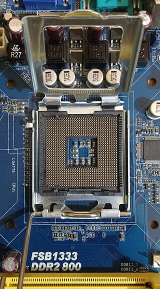
LGA 775, also known as Socket T, is an Intel desktop CPU socket. Unlike PGA CPU sockets, such as its predecessor Socket 478, LGA 775 has no socket holes; instead, it has 775 protruding pins which touch contact points on the underside of the processor (CPU).

Pentium D is a range of desktop 64-bit x86-64 processors based on the NetBurst microarchitecture, which is the dual-core variant of the Pentium 4 manufactured by Intel. Each CPU comprised two cores. The brand's first processor, codenamed Smithfield and manufactured on the 90 nm process, was released on May 25, 2005, followed by the 65 nm Presler nine months later. The core implementation on the 90 nm Smithfield and later 65 nm Presler are designed differently but are functionally the same. The 90 nm Smithfield contains a single die, with two adjoined but functionally separate CPU cores cut from the same wafer. The later 65 nm Presler utilized a multi-chip module package, where two discrete dies each containing a single core reside on the CPU substrate. Neither the 90 nm Smithfield nor the 65 nm Presler were capable of direct core to core communication, relying instead on the northbridge link to send information between the two cores.
The P6 microarchitecture is the sixth-generation Intel x86 microarchitecture, implemented by the Pentium Pro microprocessor that was introduced in November 1995. It is frequently referred to as i686. It was planned to be succeeded by the NetBurst microarchitecture used by the Pentium 4 in 2000, but was revived for the Pentium M line of microprocessors. The successor to the Pentium M variant of the P6 microarchitecture is the Core microarchitecture which in turn is also derived from P6.

Yonah is the code name of Intel's first generation 65 nm process CPU cores, based on cores of the earlier Banias / Dothan Pentium M microarchitecture. Yonah CPU cores were used within Intel's Core Solo and Core Duo mobile microprocessor products. SIMD performance on Yonah improved through the addition of SSE3 instructions and improvements to SSE and SSE2 implementations; integer performance decreased slightly due to higher latency cache. Additionally, Yonah included support for the NX bit.

Intel Core 2 is a processor family encompassing a range of Intel's mainstream 64-bit x86-64 single-, dual-, and quad-core microprocessors based on the Core microarchitecture. The single- and dual-core models are single-die, whereas the quad-core models comprise two dies, each containing two cores, packaged in a multi-chip module. The Core 2 range is the last flagship range of Intel desktop processors to use a front-side bus (FSB).

Pentium is a discontinued series of x86 architecture-compatible microprocessors produced by Intel. The original Pentium was first released on March 22, 1993. The name "Pentium" is originally derived from the Greek word pente (πεντε), meaning "five", a reference to the prior numeric naming convention of Intel's 80x86 processors (8086–80486), with the Latin ending -ium since the processor would otherwise have been named 80586 using that convention.
Platform Environment Control Interface (PECI) is an Intel proprietary single wire serial interface that provides a communication channel between Intel processors and chipset components to external system management logic and thermal monitoring devices. Also, PECI provides an interface for external devices to read processor temperature, perform processor manageability functions, and manage processor interface tuning and diagnostics. Typically in server platforms, CPUs are the PECI slaves and Platform Controller Hub (PCH) is the PECI master, meanwhile in client segment, CPU is usually the PECI slave and EC/BMC is the PECI master. PECI was introduced in 2006 with the Intel Core 2 Duo microprocessors.

The Pentium Dual-Core brand was used for mainstream x86-architecture microprocessors from Intel from 2006 to 2009, when it was renamed to Pentium. The processors are based on either the 32-bit Yonah or 64-bit Merom-2M, Allendale, and Wolfdale-3M core, targeted at mobile or desktop computers.
The P35 Express is a mainstream desktop computer chipset from Intel released in June 2007, although motherboards featuring the chipset were available a month earlier. The P35 Express chipset supports Intel's LGA 775 socket and Core 2 Duo and Quad processors, and is also known to support 45 nm Wolfdale/Yorkfield dual and quad core CPUs. Theoretically, Intel also dropped support for Intel's Pentium 4 and Pentium D processors with this chipset although late Pentium 4 processors, including both the 32-bit-only (5x0) and the 32-bit/64-bit (5x1), and a few others, were fully supported.

Haswell is the codename for a processor microarchitecture developed by Intel as the "fourth-generation core" successor to the Ivy Bridge. Intel officially announced CPUs based on this microarchitecture on June 4, 2013, at Computex Taipei 2013, while a working Haswell chip was demonstrated at the 2011 Intel Developer Forum. Haswell was the last generation of Intel processor to have socketed processors on mobile. With Haswell, which uses a 22 nm process, Intel also introduced low-power processors designed for convertible or "hybrid" ultrabooks, designated by the "U" suffix. Haswell began shipping to manufacturers and OEMs in mid-2013, with its desktop chips officially launched in September 2013.

Conroe is the code name for many Intel processors sold as Core 2 Duo, Xeon, Pentium Dual-Core and Celeron. It was the first desktop processor to be based on the Core microarchitecture, replacing the NetBurst microarchitecture based Cedar Mill processor. It has product code 80557, which is shared with Allendale and Conroe-L that are very similar but have a smaller L2 cache. Conroe-L has only one processor core and a new CPUID model. The mobile version of Conroe is Merom, the dual-socket server version is Woodcrest, the quad-core desktop version is Kentsfield and the quad-core dual-socket version is Clovertown. Conroe was replaced by the 45 nm Wolfdale processor.

Intel Core is a line of multi-core central processing units (CPUs) for midrange, embedded, workstation, high-end and enthusiast computer markets marketed by Intel Corporation. These processors displaced the existing mid- to high-end Pentium processors at the time of their introduction, moving the Pentium to the entry level. Identical or more capable versions of Core processors are also sold as Xeon processors for the server and workstation markets.

Ivy Bridge is the codename for Intel's 22 nm microarchitecture used in the third generation of the Intel Core processors. Ivy Bridge is a die shrink to 22 nm process based on FinFET ("3D") Tri-Gate transistors, from the former generation's 32 nm Sandy Bridge microarchitecture—also known as tick–tock model. The name is also applied more broadly to the Xeon and Core i7 Extreme Ivy Bridge-E series of processors released in 2013.
References
- ↑ Performance and Power Consumption Control Features in Intel Pentium 4 and Intel Xeon Processors – Different Names, the Same Principles
- ↑ Thermal Monitor 2 - Intel E2160 - CPU Pentium Dual-Core 1.80Ghz Fsb800Mhz 1M Lga775 Tray Guide (Page 28)
- ↑ Berktold, Michael; Tian, Tian (September 2010). "CPU Monitoring With DTS/PECI". Intel. Retrieved 29 April 2017.