
A transistor is a semiconductor device used to amplify or switch electrical signals and power. It is one of the basic building blocks of modern electronics. It is composed of semiconductor material, usually with at least three terminals for connection to an electronic circuit. A voltage or current applied to one pair of the transistor's terminals controls the current through another pair of terminals. Because the controlled (output) power can be higher than the controlling (input) power, a transistor can amplify a signal. Some transistors are packaged individually, but many more in miniature form are found embedded in integrated circuits. Because transistors are the key active components in practically all modern electronics, many people consider them one of the 20th century's greatest inventions.

In electronics, the metal–oxide–semiconductor field-effect transistor is a type of field-effect transistor (FET), most commonly fabricated by the controlled oxidation of silicon. It has an insulated gate, the voltage of which determines the conductivity of the device. This ability to change conductivity with the amount of applied voltage can be used for amplifying or switching electronic signals. The term metal–insulator–semiconductor field-effect transistor (MISFET) is almost synonymous with MOSFET. Another near-synonym is insulated-gate field-effect transistor (IGFET).

Complementary metal–oxide–semiconductor is a type of metal–oxide–semiconductor field-effect transistor (MOSFET) fabrication process that uses complementary and symmetrical pairs of p-type and n-type MOSFETs for logic functions. CMOS technology is used for constructing integrated circuit (IC) chips, including microprocessors, microcontrollers, memory chips, and other digital logic circuits. CMOS technology is also used for analog circuits such as image sensors, data converters, RF circuits, and highly integrated transceivers for many types of communication.

Flash memory is an electronic non-volatile computer memory storage medium that can be electrically erased and reprogrammed. The two main types of flash memory, NOR flash and NAND flash, are named for the NOR and NAND logic gates. Both use the same cell design, consisting of floating gate MOSFETs. They differ at the circuit level depending on whether the state of the bit line or word lines is pulled high or low: in NAND flash, the relationship between the bit line and the word lines resembles a NAND gate; in NOR flash, it resembles a NOR gate.

EEPROM or E2PROM (electrically erasable programmable read-only memory) is a type of non-volatile memory. It is used in computers, usually integrated in microcontrollers such as smart cards and remote keyless systems, or as a separate chip device, to store relatively small amounts of data by allowing individual bytes to be erased and reprogrammed.

An EPROM, or erasable programmable read-only memory, is a type of programmable read-only memory (PROM) chip that retains its data when its power supply is switched off. Computer memory that can retrieve stored data after a power supply has been turned off and back on is called non-volatile. It is an array of floating-gate transistors individually programmed by an electronic device that supplies higher voltages than those normally used in digital circuits. Once programmed, an EPROM can be erased by exposing it to strong ultraviolet (UV) light source. EPROMs are easily recognizable by the transparent fused quartz window on the top of the package, through which the silicon chip is visible, and which permits exposure to ultraviolet light during erasing.

Electromigration is the transport of material caused by the gradual movement of the ions in a conductor due to the momentum transfer between conducting electrons and diffusing metal atoms. The effect is important in applications where high direct current densities are used, such as in microelectronics and related structures. As the structure size in electronics such as integrated circuits (ICs) decreases, the practical significance of this effect increases.
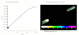
The threshold voltage, commonly abbreviated as Vth or VGS(th), of a field-effect transistor (FET) is the minimum gate-to-source voltage (VGS) that is needed to create a conducting path between the source and drain terminals. It is an important scaling factor to maintain power efficiency.
In the semiconductor industry, the term high-κ dielectric refers to a material with a high dielectric constant, as compared to silicon dioxide. High-κ dielectrics are used in semiconductor manufacturing processes where they are usually used to replace a silicon dioxide gate dielectric or another dielectric layer of a device. The implementation of high-κ gate dielectrics is one of several strategies developed to allow further miniaturization of microelectronic components, colloquially referred to as extending Moore's Law.

A VMOS transistor is a type of metal–oxide–semiconductor field-effect transistor (MOSFET). VMOS is also used to describe the V-groove shape vertically cut into the substrate material.
Charge trap flash (CTF) is a semiconductor memory technology used in creating non-volatile NOR and NAND flash memory. It is a type of floating-gate MOSFET memory technology, but differs from the conventional floating-gate technology in that it uses a silicon nitride film to store electrons rather than the doped polycrystalline silicon typical of a floating-gate structure. This approach allows memory manufacturers to reduce manufacturing costs five ways:
- Fewer process steps are required to form a charge storage node
- Smaller process geometries can be used
- Multiple bits can be stored on a single flash memory cell
- Improved reliability
- Higher yield since the charge trap is less susceptible to point defects in the tunnel oxide layer
Negative-bias temperature instability (NBTI) is a key reliability issue in MOSFETs, a type of transistor aging. NBTI manifests as an increase in the threshold voltage and consequent decrease in drain current and transconductance of a MOSFET. The degradation is often approximated by a power-law dependence on time. It is of immediate concern in p-channel MOS devices (pMOS), since they almost always operate with negative gate-to-source voltage; however, the very same mechanism also affects nMOS transistors when biased in the accumulation regime, i.e. with a negative bias applied to the gate.
Hot carrier injection (HCI) is a phenomenon in solid-state electronic devices where an electron or a “hole” gains sufficient kinetic energy to overcome a potential barrier necessary to break an interface state. The term "hot" refers to the effective temperature used to model carrier density, not to the overall temperature of the device. Since the charge carriers can become trapped in the gate dielectric of a MOS transistor, the switching characteristics of the transistor can be permanently changed. Hot-carrier injection is one of the mechanisms that adversely affects the reliability of semiconductors of solid-state devices.
SONOS, short for "silicon–oxide–nitride–oxide–silicon", more precisely, "polycrystalline silicon"—"silicon dioxide"—"silicon nitride"—"silicon dioxide"—"silicon", is a cross sectional structure of MOSFET (metal–oxide–semiconductor field-effect transistor), realized by P.C.Y. Chen of Fairchild Camera and Instrument in 1977. This structure is often used for non-volatile memories, such as EEPROM and flash memories. It is sometimes used for TFT LCD displays. It is one of CTF (charge trap flash) variants. It is distinguished from traditional non-volatile memory structures by the use of silicon nitride (Si3N4 or Si9N10) instead of "polysilicon-based FG (floating-gate)" for the charge storage material. A further variant is "SHINOS" ("silicon"—"hi-k"—"nitride"—"oxide"—"silicon"), which is substituted top oxide layer with high-κ material. Another advanced variant is "MONOS" ("metal–oxide–nitride–oxide–silicon"). Companies offering SONOS-based products include Cypress Semiconductor, Macronix, Toshiba, United Microelectronics Corporation and Floadia.
In semiconductor electronics fabrication technology, a self-aligned gate is a transistor manufacturing approach whereby the gate electrode of a MOSFET is used as a mask for the doping of the source and drain regions. This technique ensures that the gate is naturally and precisely aligned to the edges of the source and drain.

A metal gate, in the context of a lateral metal–oxide–semiconductor (MOS) stack, is the gate electrode separated by an oxide from the transistor's channel – the gate material is made from a metal. In most MOS transistors since about the mid-1970s, the "M" for metal has been replaced by polysilicon, but the name remained.
In electronics, leakage is the gradual transfer of electrical energy across a boundary normally viewed as insulating, such as the spontaneous discharge of a charged capacitor, magnetic coupling of a transformer with other components, or flow of current across a transistor in the "off" state or a reverse-polarized diode.
Electronic components have a wide range of failure modes. These can be classified in various ways, such as by time or cause. Failures can be caused by excess temperature, excess current or voltage, ionizing radiation, mechanical shock, stress or impact, and many other causes. In semiconductor devices, problems in the device package may cause failures due to contamination, mechanical stress of the device, or open or short circuits.

The field-effect transistor (FET) is a type of transistor that uses an electric field to control the flow of current in a semiconductor. It comes in two types: junction FET (JFET) and metal-oxide-semiconductor FET (MOSFET). FETs have three terminals: source, gate, and drain. FETs control the flow of current by the application of a voltage to the gate, which in turn alters the conductivity between the drain and source.
A nanoscale vacuum-channel transistor (NVCT) is a transistor in which the electron transport medium is a vacuum, much like a vacuum tube. In a traditional solid-state transistor, a semiconductor channel exists between the source and the drain, and the current flows through the semiconductor. However, in a nanoscale vacuum-channel transistor, no material exists between the source and the drain, and therefore, the current flows through the vacuum.