Related Research Articles

Photonics is a branch of optics that involves the application of generation, detection, and manipulation of light in the form of photons through emission, transmission, modulation, signal processing, switching, amplification, and sensing. Photonics is closely related to quantum electronics, where quantum electronics deals with the theoretical part of it while photonics deal with its engineering applications. Though covering all light's technical applications over the whole spectrum, most photonic applications are in the range of visible and near-infrared light. The term photonics developed as an outgrowth of the first practical semiconductor light emitters invented in the early 1960s and optical fibers developed in the 1970s.

Indium phosphide (InP) is a binary semiconductor composed of indium and phosphorus. It has a face-centered cubic ("zincblende") crystal structure, identical to that of GaAs and most of the III-V semiconductors.

University College Cork – National University of Ireland, Cork (UCC) is a constituent university of the National University of Ireland, and located in Cork.

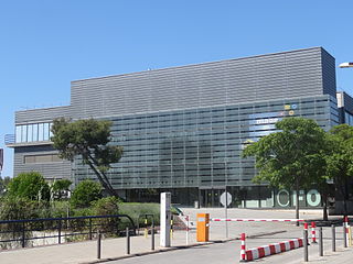
ICFO – The Institute of Photonic Sciences is a research center devoted to the science and technology of light. Located in Castelldefels, ICFO was created in 2002 by the Government of Catalonia and the Technical University of Catalonia.
The School of Engineering and Applied Science (SEAS) at the George Washington University in Washington, D.C. is a technical school which specializes in engineering, technology, communications, and transportation. The school is located on the main campus of the George Washington University and offers both undergraduate and graduate programs.
A photonic integrated circuit (PIC) or integrated optical circuit is a microchip containing two or more photonic components that form a functioning circuit. This technology detects, generates, transports, and processes light. Photonic integrated circuits use photons as opposed to electrons that are used by electronic integrated circuits. The major difference between the two is that a photonic integrated circuit provides functions for information signals imposed on optical wavelengths typically in the visible spectrum or near-infrared (850–1650 nm).
Nanoelectronics refers to the use of nanotechnology in electronic components. The term covers a diverse set of devices and materials, with the common characteristic that they are so small that inter-atomic interactions and quantum mechanical properties need to be studied extensively. Some of these candidates include: hybrid molecular/semiconductor electronics, one-dimensional nanotubes/nanowires or advanced molecular electronics.

The Max Planck Institute for the Science of Light (MPL) performs basic research in optical metrology, optical communication, new optical materials, plasmonics and nanophotonics and optical applications in biology and medicine. It is part of the Max Planck Society and was founded on January 1, 2009 in Erlangen near Nuremberg. The institute is based on the Max Planck Research Group "Optics, Information and Photonics", which was founded in 2004 at the University of Erlangen-Nuremberg, as a precursor. The institute currently comprises four divisions.

The Ferdinand-Braun-Institut, Leibniz-Institut für Höchstfrequenztechnik (FBH) is a research institute, which is a member of the Gottfried Wilhelm Leibniz Scientific Community. The institute is located in Berlin at the Wissenschafts- und Wirtschaftsstandort Adlershof (WISTA), its research activity is applied science in the fields of III-V electronics, photonics, integrated quantum technology and III-V technology
The IEEE Photonics Award is a Technical Field Award established by the IEEE Board of Directors in 2002. This award is presented for outstanding achievements in photonics, including work relating to: light-generation, transmission, deflection, amplification and detection and the optical/electro-optical componentry and instrumentation used to accomplish these functions. Also included are storage technologies utilizing photonics to read or write data and optical display technologies. It also extends from energy generation/propagation, communications, information processing, storage and display, biomedical and medical uses of light and measurement applications.
Photonics and Nanostructures: Fundamentals and Applications is a peer-reviewed scientific journal, published quarterly by Elsevier. The editors-in-chief are A. Di Falco University of St Andrews, M. Lapine University of Technology Sydney, P. Tassin Chalmers University of Technology, M. Vanwolleghem Centre National de la Recherche Scientifique (CNRS), Villeneuve-d'Ascq, and L. O'Faolain Cork Institute of Technology.

CEA-Leti is a research institute for electronics and information technologies, based in Grenoble, France. It is one of the world's largest organizations for applied research in microelectronics and nanotechnology. It is located within the CEA Grenoble center of the French Alternative Energies and Atomic Energy Commission (CEA).
The Intel Outstanding Researcher Award is presented by Intel Corporation for outstanding contributions to the development of advanced nanoelectronic and manufacturing technologies. The award was created to recognize truly outstanding contributions by researchers funded by Intel’s Corporate Research Council and associated Strategic Research Sectors (SRSs) and the inaugural awards were announced during 2012. In selecting the award winners, careful consideration is given to the fundamental insights, industrial relevance, technical difficulty, communications and potential student hiring associated with a candidate's research program.
Multi-Scale Multidisciplinary Modeling of Electronic Materials (MSME) Collaborative Research Alliance (CRA) was a research program in the United States that was initiated and sponsored by the US Army Research Laboratory (ARL). The objective of the program was “to develop quantitative understanding of materials from the smallest to the largest relevant scales to advance the state of the art in electronic, optoelectronic and electrochemical materials and devices.”

Alexandra Boltasseva is Ron And Dotty Garvin Tonjes Distinguished Professor of electrical and computer engineering at Purdue University, and editor-in-chief for The Optical Society's Optical Materials Express journal. Her research focuses on plasmonic metamaterials, manmade composites of metals that use surface plasmons to achieve optical properties not seen in nature.

John E. Bowers is an American physicist, engineer, researcher and educator. He holds the Fred Kavli Chair in Nanotechnology, the director of the Institute for Energy Efficiency and a distinguished professor in the Departments of Electrical and Computer Engineering and Materials at University of California, Santa Barbara. He was the deputy director of American Institute of Manufacturing of Integrated Photonics from 2015 to 2022.

Niels Quack is a Swiss and German engineer specialized in optical micro engineering. He is a SNSF professor at EPFL and director of the Photonic Micro- and Nanosystems Laboratory at its school of engineering.
Boon S. Ooi is a Malaysian–American academic researcher and a Professor of Electrical and Computer Engineering at King Abdullah University of Science and Technology (KAUST) in Saudi Arabia. He was faculty member at Nanyang Technological University (Singapore) from 1996 to 2000 and at Lehigh University from 2003 to 2009. He served as Director of KACST-Technology Innovation Center at KAUST from 2012 to 2020.
References
- ↑ "The Tyndall National Institute, UCC leads high tech future". www.ucc.ie. 20 May 2011. Retrieved 14 November 2019.
- ↑ "John Tyndall's blue sky apparatus". www.rigb.org. retrieved 2019-11-14
- ↑ "Our scientific genius Tyndall who was accidentally murdered by his wife". www.irishexaminer.com. 4 December 2013. retrieved 2019-11-14
- ↑ "John Tyndall - Science Communicator". retrieved 2019-11-14
- 1 2 3 4 "Tyndall National Institute - History". www.tyndall.ie. retrieved 2019-11-14
- ↑ Hogan, Dick. "NMRC extension in Cork is opened". The Irish Times. retrieved 2019-11-14
- ↑ https://www.tyndall.ie/facility-description Tyndall.ie retrieved 2/10/2019
- ↑ https://www.ucc.ie/en/research/news-events/news/tyndall-to-progress-major-expansion-under-the-governments-national-development-plan.html UCC.ie retrieved 2/10/2019
- 1 2 3 https://www.irishexaminer.com/breakingnews/business/tyndall-national-institute-secures-additional-8m-in-eu-funding-948381.html Irishexaminer.com retrieved 2/10/2019